


Features
| Applications
|
Blog
Features
| Applications
|
Absolute Maximum Ratings(1)
Unless specified otherwise, Tamb= 25℃
| Parameter | Symbol | Value | Unit |
| Supply Voltage | VDD1/VDD2 | -0.5~6 | V |
| A/B Input Voltage | VINA/VINB | -0.5~VDD1/VDD2+0.5(2) | V |
| Operating Temperature | Tamb | -40~125 | ℃ |
| Junction Temperature | TJ | 150 | ℃ |
| Storage Temperature | Tstg | -65~150 | ℃ |
| Pin Temperature(reflow soldering) | 260 | ℃ | |
| Rated Insulation with Stand Voltage | 5 | KVrms(3) |
Note: (1) If the operating conditions exceed the above “Absolute Maximum Ratings”, it may cause permanent damage to the device. The above values are only maximum values for operating conditions and we do not recommend devices to operate outside this specification. The stability of devices may be affected under absolute limit parameter conditions for a long time.
DC Electrical Characteristics
Unless specified otherwise,VDD=2.5V±5% or 3.3V±10% or 5V±10%,Tamb= 25℃
| Parameter | Symbol | Test Conditions | Min | Typ | Max | Unit |
| VDD Undervoltage threshold | VDDUV+ | VDD1, VDD2 rising up | 1.9 | 2.2 | 2.37 | V |
| VDD Undervoltage threshold | VDDUV– | VDD1, VDD2 failing down | 1.85 | 2.12 | 2.32 | V |
| VDD Undervoltage hysteresis | VDDHYS | 50 | 70 | 95 | mV | |
| Positive input threshold | VT+ | All inputs rising up | 1.4 | 1.6 | 1.9 | V |
| Reverse input threshold | VT– | All inputs failing down | 1.0 | 1.3 | 1.4 | V |
| Input Threshold Hysteresis | VHYS | 0.38 | 0.44 | 0.50 | V | |
| High Level Input Voltage | VIH | 2.0 | – | – | V | |
| Low Level Input Voltage | VIL | – | – | 0.8 | V | |
| High Level Output Voltage | VOH | loh=–4mA | VDD–0.4 | VDD–0.2 | – | V |
| Low Level Output Voltage | VOL | lol=4mA | – | 0.2 | 0.4 | V |
| Input leakage current | IL | – | – | ±10 | µA | |
| Output Impedance(1) | ZO | – | 50 | – | Ω | |
| Enable input current | IENH,IENL | VEN=VIH or VIL | – | 2.0 | – | µA |
| Data Rate | 0 | – | 150 | Mbps | ||
| Minimum Pulse Width | – | – | 5.0 | ns | ||
| Propagation Delay | tPHL,tPLH | See Figure 2 | 5.0 | 9.0 | 15 | ns |
| Pulse Width Distortion |tPLH–tPHL| | PWD | See Figure 2 | – | 0.2 | 4.5 | ns |
| Part-to-Part Delay Skew(2) | tPSK(P-P) | – | 2.0 | 4.5 | ns | |
| Channel-to-Channel Delay Skew | tPSK | – | 0.4 | 2.5 | ns | |
| Rising Time | tr | CL=15pF,See Figure 2 | – | 2.2 | 4.0 | ns |
| Falling Time | tf | CL=15pF,See Figure2 | – | 2.2 | 4.0 | ns |
| Peak Eye Diagram Jitter | tJIT(PK) | – | 350 | – | ps | |
| Common Mode Transient Immunity | CMTI | VI=VDD or 0 VCM=1500V | 35 | 50 | – | kV/µs |
| Enable to Data high Valid | ten1 | See Figure 1 | – | 5.0 | 12 | ns |
| Disable high to Tri-State | ten2 | See Figure 1 | – | 65 | 98 | us |
| Input Drop Time to Effective Output Drop Time | tSD | – | 28 | 45 | ns | |
| Startup Time(3) | tSU | – | 15 | 45 | µs |
Note: (1) The nominal output impedance of the isolator channel is approximately 50Ω±40%, which is a combination of on-chip series resistors and output FET channel resistors. When driving load, transmission line effect will be a factor affecting the signal, the output pin should be connected to impedance controlled PCB wiring.
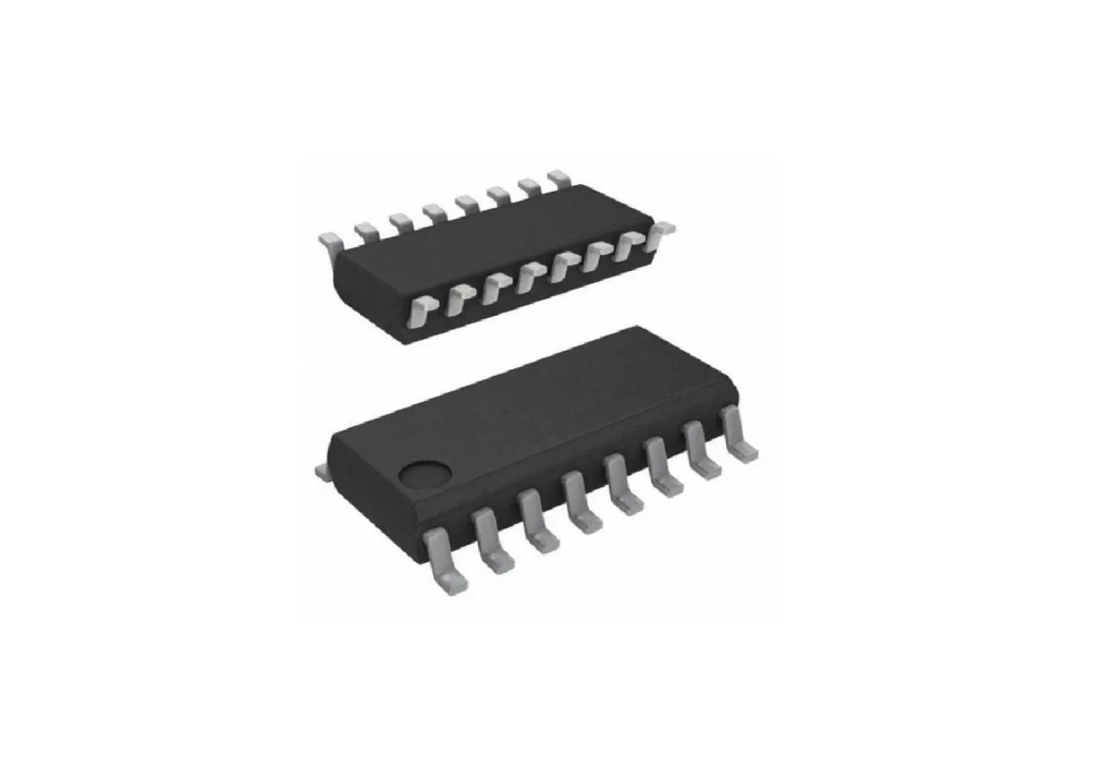
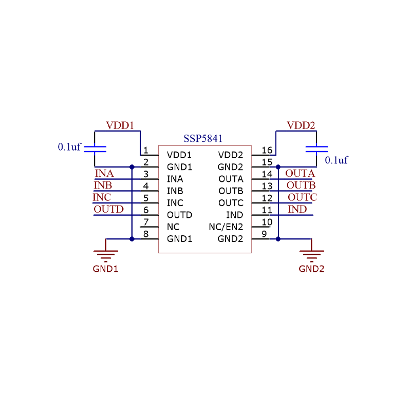
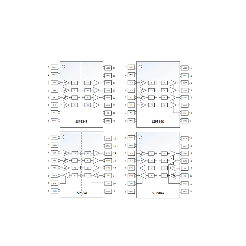
Selection Table
| Part No | The total number of channels | Number of reverse channels | Default output level | Package | Manner of Packing | Devices per reel |
| SSP5840ED | 4 | 0 | High | SOIC-16 | Reel | 2000 |
| SSP5841ED | 4 | 1 | High | SOIC-16 | Reel | 2000 |
| SSP5842ED | 4 | 2 | High | SOIC-16 | Reel | 2000 |
| SSP5845ED | 4 | 0 | High | SOIC-16 | Reel | 2000 |
| SSP5840BD | 4 | 0 | Low | SOIC-16 | Reel | 2000 |
| SSP5841BD | 4 | 1 | Low | SOIC-16 | Reel | 2000 |
| SSP5842BD | 4 | 2 | Low | SOIC-16 | Reel | 2000 |
| SSP5845BD | 4 | 0 | Low | SOIC-16 | Reel | 2000 |

_画板-1@2x.png)
Shanghai Siproin
Microelectronics Co.,Ltd.
Welcome your contact.

