
Features
| Application
|

Blog
Features
| Application
|
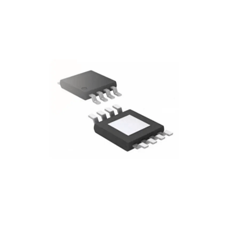
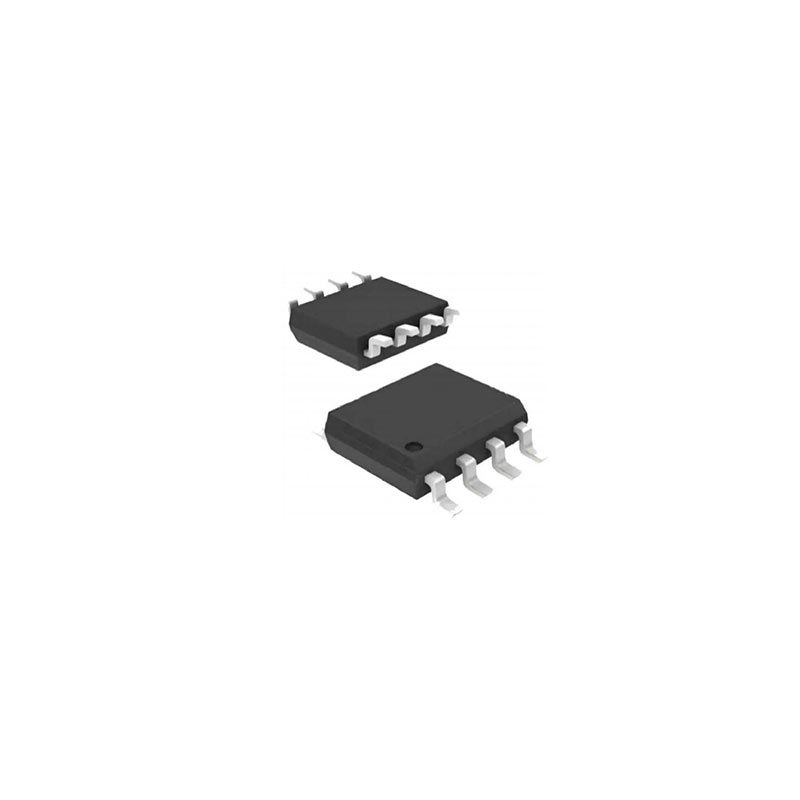
Order Information
| Part No | Package | Manner of Packing | Devices per bag/reel |
| MAX3085 | SOP8 | Reel | 4000 |
Pin Description
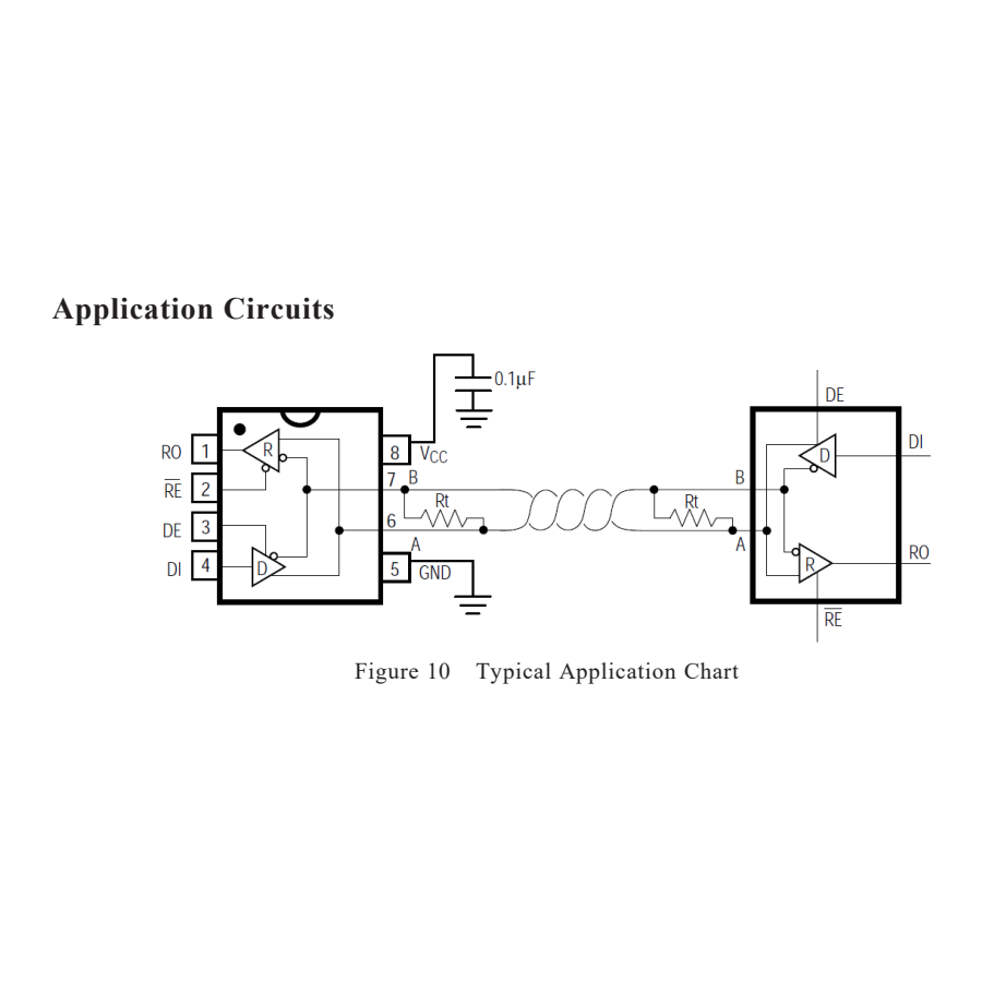
| Pin No. | Pin Name | Description | I/O |
| 1 | RO | Receiver output:If A-B≥-0.05V,RO will be high;If A-B≤-0.2V,RO will be low;If A and B are open or shorted,RO will be high. | O |
| 2 | RE | Receiver output enable:RO is enabled when RE is low;RO is high impedance when RE is high. | I |
| 3 | DE | Driver output enable:The driver outputs,A and B are enabled by bringing DE high. They are high impedance when DE is low. | I |
| 4 | DI | Driver input:A low on DI forces output A low and output B high. Similarly, a high on DI forces output A high and output B low. | I |
| 5 | GND | Ground | |
| 6 | A | Receiver input and driver output | I/O |
| 7 | B | Receiver input and driver output | I/O |
| 8 | VDD | Supply voltage |
Truth Table
| Input | Output | ||
| RE | DE | A – B | RO |
| L | X | ≥-0.05V | H |
| L | X | ≤-0.2V | L |
| L | X | Open/shorted | H |
| H | H | X | Z |
| H | L | X | Z |
Truth Table
| Input | Output | |||
| RE | DE | DI | B | A |
| X | H | H | L | H |
| X | H | L | H | L |
| L | L | X | Z | Z |
| H | L | X | Z |
Absolute Maximum Ratings
| Parameter | Symbol | Value | Unit |
| Supply Voltage | V DD | -0.5~6 | V |
| Input Voltage | V IN | -0.5~6 | V |
| Output Voltage | V OUT | GND-0.3~V +0.3 DD | V |
| A/B Input / Output Voltage | V /V INA/B OUTA/B | -7~12 | V |
| Operating Temperature | T amb | -40~85 | ℃ |
| Storage Temperature | T stg | -65~150 | ℃ |
| Soldering Temperature(10s) | T sol | 300 | ℃ |
Electrical Characteristics
| Parameter | Symbol | Test Conditions | Min | Typ | Max | Unit | |
| Driver | |||||||
| Differential driver output | V OD1 | No load | 5 | V | |||
| Differential driver output | V OD2 | R=50Ω or 27Ω(1) | 2.0 | 3.0 | V | ||
| Change in magnitude of driver differential output voltage for complementary output states | ΔV OD | R=50Ω or 27Ω(1) | 0.2 | V | |||
| Driver common-mode output voltage | V OC | R=50Ω or 27Ω(1) | V / DD 2 | 3 | V | ||
| Change in magnitude of driver common-mode output voltage for complementary output states | ΔV OC | R=50Ω or 27Ω(1) | 0.2 | V | |||
| Input high voltage | V IH1 | DE、RE、DI | 2.0 | V | |||
| Input low voltage | V IL1 | DE、RE、DI | 0.8 | V | |||
| Input current | I IN1 | DE、RE、DI | ±2 | A | |||
| Input current (A, B) | I IN2 | DE=GND,V = 5V CC | Vin=5V | 40 | 90 | A | |
| Vin=-0V | 60 | 100 | A | ||||
| Receiver | |||||||
| Differential threshold voltage | V TH | -7V≤V ≤12V CM | -250 | -10 | mV | ||
| input hysteresis voltage | ΔV TH | 25 | mV | ||||
| output high voltage | V OH | I =-4mA O | V – CC 1.5 | V | |||
| output low voltage | V OL | I =4mA O | 0.4 | V | |||
| 3-state(high impedance) output current at receiver | I OZR | 0.4V≤V ≤2.4V O | 1 | A | |||
| input resistance | R IN | -7V≤V ≤12V CM | 96 | kΩ | |||
| Receiver short-circuit current | I OSR | 0V≤V ≤V RO DD | 80 | mA | |||
| Supply Current | I CC | No load,RE=DI =GND or V DD | DE=V DD | 480 | 800 | A | |
| DE=GND | 450 | 700 | A | ||||
| ESD Protection(A/B) | ESD | Human Body Model | 15 | kV |
Electrical Characteristics
| Parameter | Symbol | Test Conditions | Min. | Typ. | Max. | Unit |
| Driver Input to Output | t DPLH | R =50Ω,DIFF C =C =100pF(3)(6) L1 L2 | 250 | 1000 | ns | |
| Driver Input to Output | t DPHL | R =50Ω,DIFF C =C =100pF(3)(6) L1 L2 | 250 | 1000 | ns | |
| |t -t | DPLH DPHL | t DSKEW | R =50Ω,DIFF CL1=CL2=100pF(3)(6) | -3 | ±100 | ns | |
| Driver Rise or Fall Time | t, t DR DF | R =50Ω,DIFF C =C =100pF(3)(6) L1 L2 | 200 | 750 | ns | |
| Maximum Data Rate | f MAX | 1 | Mbps | |||
| Driver Enable to Output High | t DZH | C =100pF,S2 closed(4)(7) L | 2500 | ns | ||
| Driver Enable to Output Low | t DZL | C =100pF,S1 closed(4)(7) L | 2500 | ns | ||
| Driver Disable Time from Low | t DLZ | C =15pF,S1 closed(4)(7) L | 100 | ns | ||
| Driver Disable Time from Low | t DHZ | C =15pF,S2 closed(4)(7) L | 100 | ns | ||
| Receiver Input to Output | t RPLH | |V |≥2.0V ID Rise or Fall Time≤15ns(5)(8) | 200 | ns | ||
| Receiver Input to Output | t RPHL | 200 | ns | |||
| |t -t | RPLH RPHL | t RSKD | |V |≥2.0V ID Rise or Fall Time≤15ns(5)(8) | 3 | 30 | ns | |
| Receiver Enable to Output Low | t RZL | C =100pF,S1 closed(2)(9) L | 20 | 50 | ns | |
| Receiver Enable to Output High | t RZH | C =100pF,S2 closed(2)(9) L | 20 | 50 | ns | |
| Receiver Disable Time from Low | t RLZ | C =100pF,S1 closed(2)(9) L | 20 | 50 | ns | |
| Receiver Disable Time from High | t RHZ | C =100pF,S2 closed(2)(9) L | 20 | 50 | ns |