


Features
| Applications
|
_画板-1@2x.png)
Blog
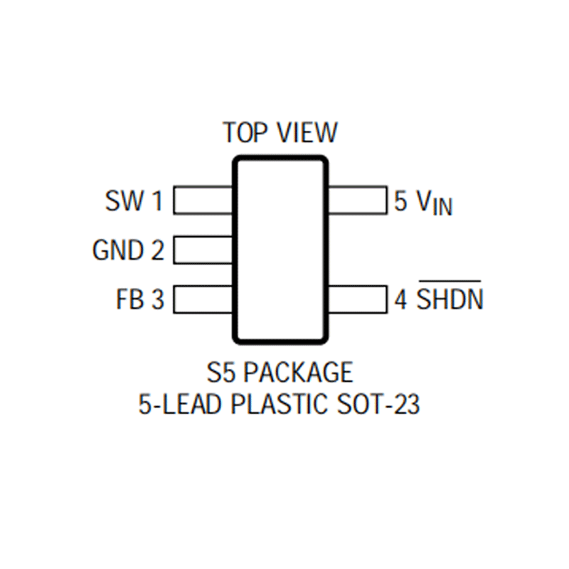
Features
| Applications
|
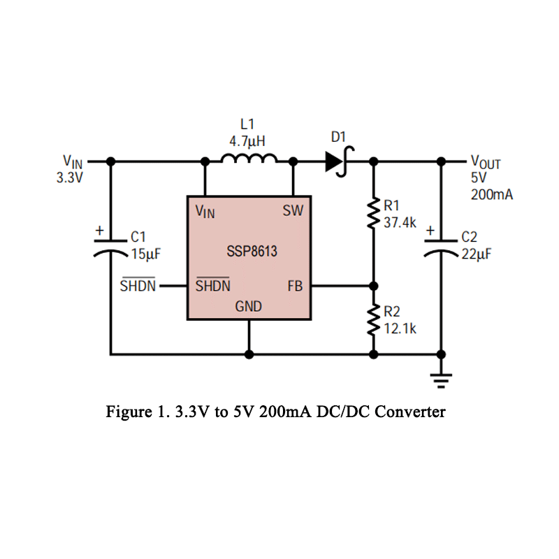
Absolute Maximum Ratings
| VIN Voltage | 10V |
| SW Voltage | – 0.4V to 36V |
| FB Voltage | VIN + 0.3V |
| Current into FB Pin | ±1mA |
| SHDN Voltage | 10V |
| Maximum Junction Temperature | 125°C |
| Operating Temperature Range | –40° C to 85° |
Electrical Characteristics
The ● denotes the specifications which apply over the full operatin temperature range, otherwise specifications are at TA = 25° C.VIN = 1.5V, VSHDN = VIN unless otherwise noted.
| PARAMETER | CONDITIONS | MIN | TYP | MAX | UNITS | |
| Minimum Operating Voltage | 1.2 | V | ||||
| Maximum Operating Voltage | 10 | V | ||||
| Feedback Voltage | ● | 1.200 | 1.23 | 1.260 | V | |
| FB Pin Bias Current | ● | 27 | 80 | nA | ||
| Quiescent Current | 3 | 4.5 | mA | |||
| Quiescent Current in Shutdown | VSHDN=0V,VIN=2V VSHDN=0V,VIN=5V | 0.01 0.01 | 0.5 1.0 | μA μA | ||
| Reference Line Regulation | 1.5V ≤ V IN ≤ 10V | 0.02 | 0.2 | %/V | ||
| Switching Frequency | ● | 2.0 | MHz | |||
| Maximum Duty Cycle | ● | 82 | 86 | % | ||
| Switch Current Limit | (Note 2) | 550 | 800 | mA | ||
| Switch VCESAT | ISW = 300mA | 300 | 350 | mV | ||
| Switch Leakage Current | VSW = 5V | 0.01 | 1 | μA | ||
| SHDN Input Voltage High | 1 | V | ||||
| SHDN Input Voltage Low | 0.3 | V | ||||
| SHDN Pin Bias Current | VSHDN=3V VSHDN=0V | 25 0.01 | 50 0.1 | μA μA | ||
Note 1: Absolute Maximum Ratings are those values beyond which the life of a device maybe impaired.
Note 2: Current limit guaranteed by design and/or correlation to static test.
Shanghai Siproin
Microelectronics Co.,Ltd.
Welcome your contact.

