
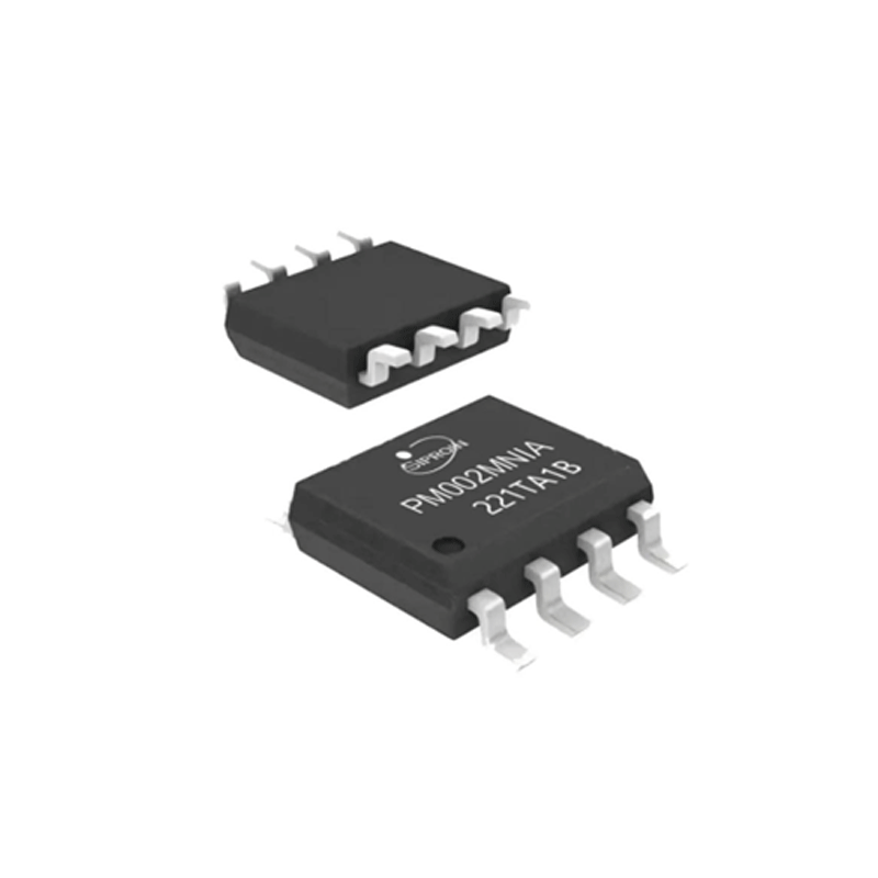
Features
| Applications
|
_画板-1@2x.png)
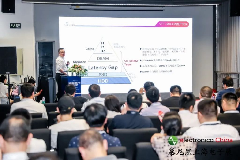
Blog

Features
| Applications
|
Absolute Maximum Ratings
| Parameter name | Symbolic | Value | Unit |
| Chip Supply Voltage | VDD | -0.3~+7 | V |
| Analogue Signal Inputs | IAP, IBP, ICP, VAP, VBP, VCP to GND Voltage | -6~+6 | V |
| Reference Input Voltage | -0.3~VDD+0.3 | V | |
| Digital Input Voltage | -0.3~VDD+0.3 | V | |
| Digital Output Voltages | -0.3~VDD+0.3 | V | |
| Operating Temperature Range | T | -40~+85 | ℃ |
| Storage Temperature Range | Tstg | -40~+85 | ℃ |
| Junction Temperature | Tj | +150 | ℃ |
| SSOP24Package Power Dissipation | Pd | 450 | mW |
| Thermal Resistance | θJA | 112 | ℃/W |
| Vapour Phase Welding(60S) | +215 | ℃ | |
| Infrared Welding(15S) | +220 | ℃ |
Note:Unless otherwise specified, TA = 25℃.
Electrical Characteristics
| Measurement items | Symbolic | Measurement Conditions | Min | Typical | Max | Unit |
| Chip Operating Voltage | VDD | 4.75 | 5 | 5.25 | V | |
| Chip Working Current | IDD | 5 | 6.5 | 8 | mA | |
| Measurement error of the current channel | Channel 2 is full input (±500mV), +25℃, dynamic range 500:1 | 0.1 | % | |||
| Phase error between current and voltage channels | Line frequency 45-65Hz, V1 overrun by 37°(PF=0.8 capacitive) | ±0.1 | % | |||
| Line frequency 45-65Hz,, V1 hysteresis 60° (PF = 0.5 inductive) | ±0.1 | % | ||||
| AC power supply suppresses output frequency variations(CF) | SCF=0,S1=S0=1, IA=IB=IC=100mVrms,50Hz VA=VB=VC=100mVrms,50Hz VDD plus 200 mV rms, 100Hz ripple | 0.2 | % | |||
| DC power supply suppresses output frequency variations(CF) | S1=1,S0=SCF=0 IA=IB=IC=100mV rms,50Hz VA=VB=VC=100mVrms,50Hz VDD =5V±250mV | ±0.3 | % | |||
| Analogue Inputs | ||||||
| Max Signal Level | VA, VB, VC, IA, IB, IC voltage to GND | ±0.5 | V | |||
| DC Input Resistance | CLKOSC=10MHz | 390 | kΩ | |||
| -3dB bandwidths | CLKOSC/256,CLKOSC=10MHz | 14 | KHZ | |||
| ADC misalignment error | ±16 | mV | ||||
| Gain error | External Reference Source 2.5V,IAP=IBP=ICP=500mV ,dc | ±9 | % | |||
| On-chip Reference Source | ||||||
| Reference Voltage Error | Nominal Value 2.5V | ±200 | mV | |||
| Temperature Coefficient | Nominal Value 2.5V | 30 | ppm/℃ | |||
| Clock Input | ||||||
| Input Clock Frequency | All indicator CLKOSCs are 10MHz | 8 | 10 | 12 | MHZ | |
| logical input SCF,S0,S1,AC/DC,RESET,G0 and G1 | ||||||
| Input High Level | VINH | VDD=5V±5% | 2.4 | |||
| Input Low Level | VINL | VDD=5V±5% | 0.8 | |||
| Input Current | VIN=0V~VDD | 0.01 | ±3 | μA | ||
| Input capacitance | 10 | pF | ||||
| logical output F1,F2 | ||||||
| Output High Level | VOH | ISOURCE=10mA,VDD=5V | 4.5 | V | ||
| Output Low Level | VOL | ISINK=10mA,VDD=5V | 0.5 | V | ||
| CF,REVP | ||||||
| Output High Level | VOH | ISOURCE=10mA,VDD=5V | 4 | V | ||
| Output Low Level | VOL | ISINK=10mA,VDD=5V | 0.5 | V | ||
Noted:Unless otherwise specified, TA = 25℃.
All voltage values use the GND terminal potential a a reference point.
VDD= 5V±5%, GND=0V, using on-chip reference source, CLKOSC=10MHz.
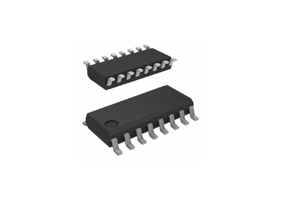
Order information
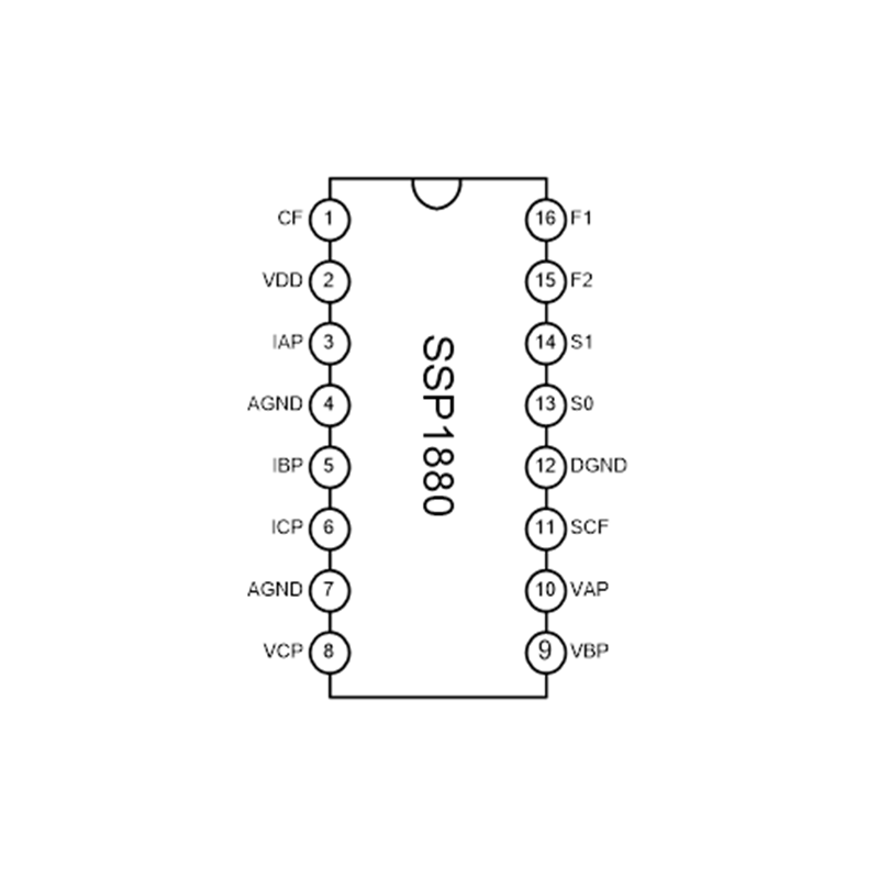
| Product model | Package | Manner of packing | Min packing quantity |
| SSP1880 | SOP16 | Reels | 2500PCS |

Shanghai Siproin
Microelectronics Co.,Ltd.
Welcome your contact.

