Electrical Characteristics
This device contains circuitry to protect the inputs against damage caused by high static voltages or electric fields. However, it is advised that normal precautions be taken to avoid application of any voltage greater than maximum rated voltages to these high-impedance (Hi-Z) circuits.
The device also contains protection against external magnetic fields. Precautions should be taken to avoid application of any magnetic field more intense than the maximum field intensity specified in the maximum ratings.
| Symbol | Parameter | Conditions | Value | Unit |
| Vcc | Supply Voltage | -0.5 to 4 | V |
| Vin | Voltage on any pin | -0.5 to Vcc | V |
| Iout | Output current per pin | ±4 | mA |
| Tbias | Temperature under bias | Commercial Grade | -40 to 85 | ℃ |
| Tstg | Storage Temperature | -55 to 125 | ℃ |
| Tlead | Lead temperature during solder(3mins max)(note1) | 260 | ℃ |
| Hmax_write | Maximum magnetic field during write | Write | 4,000 | A/m |
| Hmax_read | Maximum magnetic field during read or standby | Read or Standby | 40,000 | A/m |
| Hmax_poweroff | Maximum magnetic field during power off | Power off | 40,000 | A/m |
*Note1:We recommend programming of the device after reflow. Data written before reflow cannot be guaranteed
WARNING:Semiconductor devices can be permanently damaged by application of stress (voltage, current, temperature, magnetic etc.) in excess of absolute maximum ratings. Do not exceed these ratings.Always use semiconductor devices within their recommended operating condition ranges. Operation outside these ranges may adversely affect reliability and could result in device failure. No warranty is made with respect to uses, operating conditions, or combinations not represented on the data sheet.
DC/AC characteristic
This section presents the DC and AC characteristics of the device. The values for the DC and AC parameters indicated in the following tables are derived from tests under the operating and measurement conditions also indicated in the relevant tables. Designers should be aware that the operating conditions in their circuit match the measurement conditions when relying on the quoted parameters.
Operating Conditions
| Symbol | Parameter | Min | Max | Unit |
| Vcc | Voltage Supply | 2.7 | 3.6 | V |
| Tax | Operating Temperature(commercial) | -40 | 85 | ℃ |
DC Characteristics
| Symbol | Parameter | Test Conditions | Min | Typ. | Max | Unit |
| ILI | Input leakage current | | | | ±1 | μA |
| ILO | Output Leakage current | | | | ±1 | μA |
| ISLP | Sleep Current | | | 2 | 13 | uA |
| ISBY | Standby current | | | 2 | 2.7 | mA |
| ICC | Active Current | SPI Write/Read | CLK = 1MHz | | 2.25 | | mA |
| CLK = 10MHz | | 2.5 | | mA |
| CLK = 20MHz | | 3 | 4.8 | mA |
| CLK = 50MHz | | 4.3 | 6.9 | mA |
| QPI Write/Read | CLK = 1MHz | | 2.5 | | mA |
| CLK = 10MHz | | 4 | | mA |
| CLK = 20MHz | | 5 | 7 | mA |
| CLK = 50MHz | | 7 | 9 | mA |
| VIL | Input low voltage | | -0.3 | | 0.8 | V |
| VIH | Input high voltage | | 2.0 | | Vcc+0.3 | V |
| VOL | Output low voltage | IOL = 4mA | | | 0.4 | V |
| VOH | Output high voltage | IOH = -4mA | 2.4 | | | V |
Pin Capacitance
| Symbol | Parameter | Typical | Max | Unit |
| Cp* | VCC/VSS power external capacitance | | 10 | uF |
| CIN | Control input capacitance | – | 8 | pF |
| CIO | IO capacitance | – | 12 | pF |
| CLOAD | Load capacitance | – | 32 | рF |
*Note: The external capacitor Cp at the Vcc/Vss is recommended ≤10μF; If Cp > 10μF, reading datas may be unstable when Vcc return to the normal operating voltage from power down. In this case, for the datas are read reliably, suggest to operate the highest address to write ID(0x29, 0x55 ) data within the specified working voltage range, and then confirm this ID data before operating on the chip. If the ID data is wrong, need to send 0xB9 (sleep) and 0xAB (wake-up),so the chip will be read reliably; Otherwise, when power up and down frequently, the hardware circuit ensures that the chip starting voltage is lower than Vs (0.3V), when Vcc up from down.
AC Characteristics
| Symbol | Parameter | 50Mhz | Unit |
| Min | Max |
| tCLK | CLK period | 20 | | ns |
| tCH/tCL | Clock high/low width | 1.5 | | ns |
| tKHKL | CLK rise or fall time | | 1.5 | ns |
| tCPH | CE# High between subsequent burst | 20 | | ns |
| tCSP | CE# Setup time to CLK rising edge | 3 | | ns |
| tCHD | CE# Hold time from CLK rising edge | 50 | | ns |
| tSP | Setup time to active CLK edge | 2 | | ns |
| tHD | Hold time from active CLK edge | 2 | | ns |
| tHZ | Chip disable to DQ output high-Z | | 6 | ns |
| tACLK | CLK to output delay | 8 | 10 | ns |
| tKOH | Data hold time from clock falling edge | 1.5 | | ns |
| tRST | Reset recovery time after Operation command | 150 | | us |
| tESLP | Sleep entry time from Sleep command | | 40 | us |
| tRSLP | Recovery time from Sleep exit command | 1 | | ms |
Power Up Timing
To provide protection for data during initial power up, power loss or brownout, when ever Vcc falls below VCC(min)the device cannot be selected (CE# is restricted from going low) and the device is inhibited from Read or Write operations.
Power Up Delay Time
During initial power up or when recovering from brownout or power loss, a power up delay time (tPU) must be added from their specified minimum voltages (Vcc(min)) to normal operations may commence.This time is required to insure that the device internal voltages have stabilized.
tPU is measured from the time that Vcc have reached their specified minimum voltages. and the device will finish fuse-recall and analog blocks are stable to work.
| Symbol | Parameter | Min | Max | Unit |
| Vs | Chip Starting Voltage | – | 0.3 | V |
| t PU | Power Up delay time | 1.5 | – | ms |

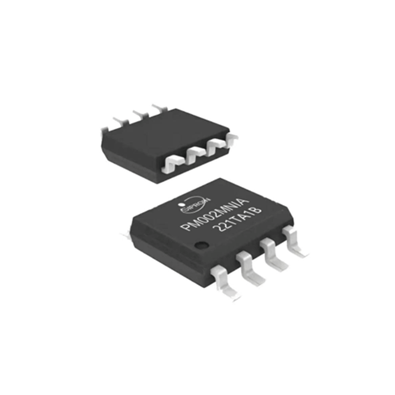
Order Information
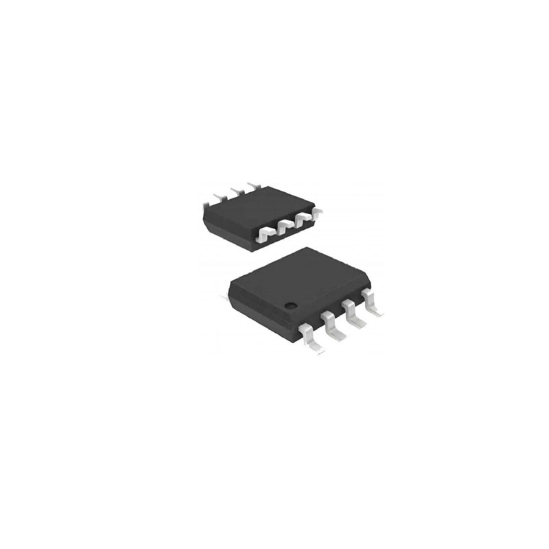
| Orderable Device | Density | Typical voltage | Interface | Package Type | Op Temp(℃) | Package Qty |
| PM004MNIATU | 4Mbit | 3.3V | SPI/QPI | SOP8_150mil | -40 to 85 | 100/Tube |
| PM004MNIATR | 4Mbit | 3.3V | SPI/QPI | SOP8_150mil | -40 to 85 | 2500/Reel |
| PM004MNIATT | 4Mbit | 3.3V | SPI/QPI | SOP8_150mil | -40 to 85 | 480/Tray |
_画板-1@2x.png)