
Características
| Aplicación
|
_画板-1@2x.png)
Blog

Características
| Aplicación
|
Especificación del pedido
| Nº de pieza | El número total de canales | Número de canales inversos | Nivel de salida por defecto | Paquete | Forma de envasado | Dispositivos por bobina |
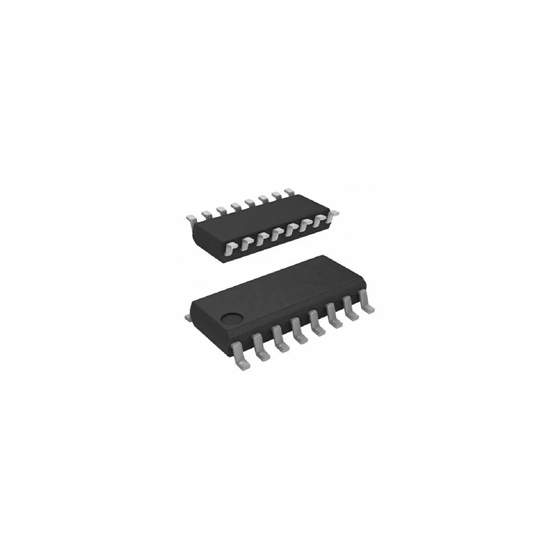
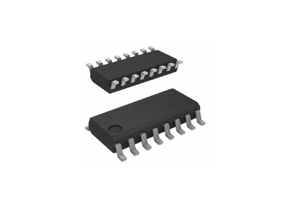
| SSP5820ED | 2 | 0 | Alta | SOIC-16 | Carrete | 2000 |
| SSP5821ED | 2 | 1 | Alta | SOIC-16 | Carrete | 2000 |
| SSP5822ED | 2 | 1 | Alta | SOIC-16 | Carrete | 2000 |
| SSP5820BD | 2 | 0 | Bajo | SOIC-16 | Carrete | 2000 |
| SSP5821BD | 2 | 1 | Bajo | SOIC-16 | Carrete | 2000 |
| SSP5822BD | 2 | 1 | Bajo | SOIC-16 | Carrete | 2000 |
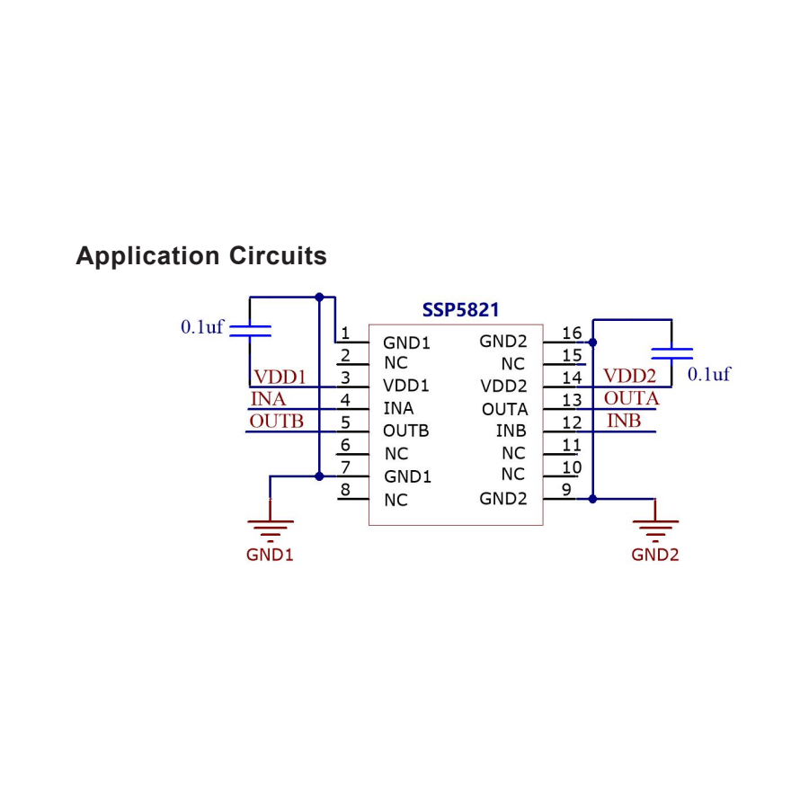
| Pin No. | Pin Name | Descripción |
| 1 | GND1 | Ground 1 |
| 2 | NC | – |
| 3 | VDD1 | Supply voltage 1 |
| 4 | INA | Digital signal input channel A |
| 5 | INB | Digital signal input channel B |
| 6 | NC | – |
| 7 | GND1 | Ground 1 |
| 8 | NC | – |
| 9 | GND2 | Ground 2 |
| 10 | NC | – |
| 11 | NC | – |
| 12 | OUTB | Digital signal output channel B |
| 13 | OUTA | Digital signal output channel A |
| 14 | VDD2 | Supply voltage 2 |
| 15 | NC | – |
| 16 | GND2 | Ground 2 |
| Pin No. | Pin Name | Descripción |
| 1 | GND1 | Ground 1 |
| 2 | NC | – |
| 3 | VDD1 | Supply voltage 1 |
| 4 | INA | Digital signal input channel A |
| 5 | OUTB | Digital signal output channel B |
| 6 | NC | – |
| 7 | GND1 | Ground 1 |
| 8 | NC | – |
| 9 | GND2 | Ground 2 |
| 10 | NC | – |
| 11 | NC | – |
| 12 | INB | Digital signal input channel B |
| 13 | OUTA | Digital signal output channel A |
| 14 | VDD2 | Supply voltage 2 |
| 15 | NC | – |
| 16 | GND2 | Ground 2 |
| Pin No. | Pin Name | Descripción |
| 1 | GND1 | Ground 1 |
| 2 | NC | – |
| 3 | VDD1 | Supply voltage 1 |
| 4 | OUTA | Digital signal output channel A |
| 5 | INB | Digital signal input channel B |
| 6 | NC | – |
| 7 | GND1 | Ground 1 |
| 8 | NC | – |
| 9 | GND2 | Ground 2 |
| 10 | NC | – |
| 11 | NC | – |
| 12 | OUTB | Digital signal output channel B |
| 13 | INA | Digital signal input channel A |
| 14 | VDD2 | Supply voltage 2 |
| 15 | NC | – |
| 16 | GND2 | Ground 2 |
Valores máximos absolutos
| Parámetro | Símbolo | Valor | Unidad |
| Tensión de alimentación | VDD1/VDD2 | -0.5~6 | V |
| A/B Input Voltage | V /V INA INB | -0.5~VDD1/VDD2+0.5(2) | V |
| Temperatura de funcionamiento | T amb | -40~125 | ℃ |
| Temperatura de unión | T J | 150 | ℃ |
| Temperatura de almacenamiento | T stg | -65~150 | ℃ |
| Pin Temperature(reflow soldering) | 260 | ℃ | |
| Rated Insulation with Stand Voltage | 5 | KVrms(3) |
Valores máximos absolutos
| Parámetro | Símbolo | Min. | Tipo. | Max. | Unidad |
| Temperatura de funcionamiento | T A | -40 | 25 | 125 | ℃ |
| Tensión de alimentación | VDD1 | 2.5 | – | 5.5 | V |
| Tensión de alimentación | VDD2 | 2.5 | – | 5.5 | V |
Valores máximos absolutos
| Parámetro | Símbolo | Condiciones de la prueba | Min | Tipo | Max | Unidad |
| VDD Undervoltage threshold | VDD UV+ | V, V rising up DD1 DD2 | 1.9 | 2.2 | 2.37 | V |
| VDD Undervoltage threshold | VDD UV– | V, V failing down DD1 DD2 | 1.85 | 2.12 | 2.32 | V |
| VDD Undervoltage hysteresis | VDD HYS | 50 | 70 | 95 | mV | |
| Umbral de entrada positivo | V T+ | Todas las entradas suben | 1.4 | 1.6 | 1.9 | V |
| Umbral de entrada inversa | V T– | Todas las entradas fallan | 1.0 | 1.3 | 1.4 | V |
| Histéresis del umbral de entrada | V HYS | 0.38 | 0.44 | 0.50 | V | |
| Tensión de entrada de nivel alto | V IH | 2.0 | - | - | V | |
| Tensión de entrada de bajo nivel | V IL | - | - | 0.8 | V | |
| Tensión de salida de alto nivel | V OH | loh=-4mA | VDD –0.4 | VDD –0.2 | - | V |
| Tensión de salida de bajo nivel | V OL | lol=4mA | - | 0.2 | 0.4 | V |
| Corriente de fuga de entrada | I L | - | - | ±10 | µA | |
| Output Impedance(1) | Z O | - | 50 | - | Ω | |
| Velocidad de datos | 0 | - | 150 | Mbps | ||
| Ancho de pulso mínimo | - | - | 5.0 | ns | ||
| Retardo de propagación | t, t PHL PLH | Véase la figura 2 | 5.0 | 9.0 | 15 | ns |
| Pulse Width Distortion |t –t | PLH PHL | PWD | Véase la figura 2 | - | 0.2 | 4.5 | ns |
| Part-to-Part Delay Skew(2) | t PSK(P-P) | - | 2.0 | 4.5 | ns | |
| Channel-to-Channel Delay Skew | t PSK | - | 0.4 | 2.5 | ns | |
| Hora de salida | tr | CL=15pF, See Figure 2 | - | 2.2 | 4.0 | ns |
| Tiempo de caída | tf | CL=15pF, See Figure2 | - | 2.2 | 4.0 | ns |
| Diagrama de ojo de pico Jitter | t JIT(PK) | - | 350 | - | ps | |
| Common Mode Transient Immunity | CMTI | VI=VDD or 0 VCM=1500V | 35 | 50 | - | kV/µs |
| Tiempo de caída de entrada a tiempo de caída de salida efectivo | t SD | - | 28 | 45 | ns | |
| Startup Time(3) | t SU | - | 15 | 45 | µs |
| VDD1 status | VDD2 status | Entrada | Salida | Comment |
| P | P | H | H | Normal operation. |
| P | P | L | L | |
| P | P | X | Hi-Z | Output Disabled, the output is high impedance |
| UP | P | X | L H | Failsafe mode, the output is default. When the input power is powered on again, the signal output responds synchronously with the signal input within 1us. |
| UP | P | X | Hi-Z | Output Disabled, the output is high impedance |
| Parámetro | Símbolo | Condiciones de la prueba | Min | Tipo | Max | Unidad |
| Retardo de propagación | t, t PHL PLH | 5.0 | 9.0 | 15 | ns | |
| Pulse Width Distortion |t –t | PLH PHL | PWD | - | 0.2 | 4.5 | ns | |
| Hora de salida | tr | CL=15pF | - | 2.2 | 4.0 | ns |
| Tiempo de caída | tf | CL=15pF | - | 2.2 | 4.0 | ns |
| Nº de pieza | Símbolo | Parámetro | Condiciones de la prueba | Min | Tipo | Max | Unidad |
| SSP5820Bx, Ex | V DD1 | Power Supply 1 | VI = 0(Bx), 1(Ex) | - | 0.9 | 1.5 | mA |
| V DD2 | Power Supply 2 | VI = 0(Bx), 1(Ex) | - | 1.5 | 2.3 | ||
| V DD1 | Power Supply 1 | VI = 1(Bx), 0(Ex) | - | 3.4 | 5.5 | ||
| V DD2 | Power Supply 2 | VI = 1(Bx), 0(Ex) | - | 1.5 | 2.4 | ||
| SSP5821/2Bx, Ex | V DD1 | Power Supply 1 | VI = 0(Bx), 1(Ex) | - | 1.4 | 2.0 | mA |
| V DD2 | Power Supply 2 | VI = 0(Bx), 1(Ex) | - | 1.4 | 2.0 | ||
| V DD1 | Power Supply 1 | VI = 1(Bx), 0(Ex) | - | 2.5 | 3.9 | ||
| V DD2 | Power Supply 2 | VI = 1(Bx), 0(Ex) | - | 2.5 | 3.9 |
| Nº de pieza | Símbolo | Parámetro | Condiciones de la prueba | Min | Tipo | Max | Unidad |
| SSP5820Bx, Ex | V DD1 | Power Supply 1 | 1Mbps Power supply current (all inputs with 500 kHz rectangular wave, all outputs with CL=15pF) | – | 2.2 | 3.2 | mA |
| V DD2 | Power Supply 2 | – | 1.7 | 2.5 | |||
| SSP5821/2Bx, Ex | V DD1 | Power Supply 1 | – | 2.0 | 3.0 | mA | |
| V DD2 | Power Supply 2 | – | 2.0 | 3.0 | |||
| SSP5820Bx, Ex | V DD1 | Power Supply 1 | 10Mbps Power supply current (all inputs with 5MHz rectangular wave, all outputs with CL=15pF) | – | 2.2 | 3.2 | mA |
| V DD2 | Power Supply 2 | – | 2.3 | 3.4 | |||
| SSP5821/2Bx, Ex | V DD1 | Power Supply 1 | – | 2.3 | 3.4 | mA | |
| V DD2 | Power Supply 2 | – | 2.3 | 3.4 | |||
| SSP5820Bx, Ex | V DD1 | Potencia | 100Mbps Power | – | 2.2 | 3.2 | mA |
| Supply 1 | supply current (all inputs with 50MHz rectangular wave, all outputs with CL=15pF) | ||||||
| V DD2 | Power Supply 2 | — | 9.0 | 12.6 | |||
| SSP5821/2Bx, Ex | V DD1 | Power Supply 1 | – | 5.9 | 8.2 | mA | |
| V DD2 | Power Supply 2 | – | 5.9 | 8.2 |
| Nº de pieza | Símbolo | Parámetro | Condiciones de la prueba | Min | Tipo | Max | Unidad |
| SSP5820Bx, Ex | V DD1 | Power Supply 1 | 1Mbps Power supply current (all inputs with 500 kHz rectangular wave, all outputs with CL=15pF) | – | 2.2 | 3.2 | mA |
| V DD2 | Power Supply 2 | – | 1.7 | 2.5 | |||
| SSP5821/2Bx, Ex | V DD1 | Power Supply 1 | – | 2.0 | 3.0 | mA | |
| V DD2 | Power Supply 2 | – | 2.0 | 3.0 | |||
| SSP5820Bx, Ex | V DD1 | Power Supply 1 | 10Mbps Power supply current (all inputs with 5MHz rectangular wave, all outputs with CL=15pF) | – | 2.2 | 3.2 | mA |
| V DD2 | Power Supply 2 | – | 2.0 | 2.9 | |||
| SSP5821/2Bx, Ex | V DD1 | Power Supply 1 | – | 2.1 | 3.1 | mA | |
| V DD2 | Power Supply 2 | – | 2.1 | 3.1 | |||
| SSP5820Bx, Ex | V DD1 | Power Supply 1 | 100Mbps Power supply current (all inputs with 50MHz rectangular wave, all outputs with CL=15pF) | – | 2.2 | 3.2 | mA |
| V DD2 | Power Supply 2 | — | 6.4 | 8.9 | |||
| SSP5821/2Bx, Ex | V DD1 | Power Supply 1 | – | 4.5 | 6.2 | mA | |
| V DD2 | Power Supply 2 | – | 4.5 | 6.2 |
| Nº de pieza | Símbolo | Parámetro | Condiciones de la prueba | Min | Tipo | Max | Unidad |
| SSP5820Bx, Ex | V DD1 | Power Supply 1 | 1Mbps Power supply current (all inputs with 500 kHz rectangular wave, all outputs with CL=15pF) | – | 2.2 | 3.2 | mA |
| V DD2 | Power Supply 2 | – | 1.7 | 2.5 | |||
| SSP5821/2Bx, Ex | V DD1 | Power Supply 1 | – | 2.0 | 3.0 | mA |
| V DD2 | Power Supply 2 | – | 2.0 | 3.0 | |||
| SSP5820Bx, Ex | V DD1 | Power Supply 1 | 10Mbps Power supply current (all inputs with 5MHz rectangular wave, all outputs with CL=15pF) | – | 2.2 | 3.2 | mA |
| V DD2 | Power Supply 2 | – | 1.8 | 2.7 | |||
| SSP5821/2Bx, Ex | V DD1 | Power Supply 1 | – | 2.1 | 3.0 | mA | |
| V DD2 | Power Supply 2 | – | 2.1 | 3.0 | |||
| SSP5820Bx, Ex | V DD1 | Power Supply 1 | 100Mbps Power supply current (all inputs with 50MHz rectangular wave, all outputs with CL=15pF) | – | 2.2 | 3.2 | mA |
| V DD2 | Power Supply 2 | — | 5.2 | 7.2 | |||
| SSP5821/2Bx, Ex | V DD1 | Power Supply 1 | – | 3.8 | 5.3 | mA | |
| V DD2 | Power Supply 2 | – | 3.8 | 5.3 |
Paquete
| Símbolo | Min.(mm) | Max.(mm) |
| A | – | 2.65 |
| A1 | 0.10 | 0.3 |
| A2 | 2.05 | – |
| b | 0.31 | 0.51 |
| c | 0.20 | 0.33 |
| D | 10.30 BSC | |
| E | 10.30 BSC | |
| E1 | 7.50 BSC | |
| e | 1.27 BSC | |
| L | 0.40 | 1.27 |
| h | 0.25 | 0.75 |
| θ | 0° | 8° |
| Note: 10. All sizes are in millimeters unless otherwise noted. 11. Dimensions and tolerances according to ANSI Y14.5M-1994. |
| Statement |
Shanghai Siproin
Microelectronics Co.,Ltd.
Su contacto es bienvenido.

