_画板-1@2x.png)

Ⅰ、 Three-wire PT100 temperature measurement principle
The core purpose of the three-wire connection method is to eliminate the influence of lead resistance on measurement accuracy. The resistance value of the PT100 is very small (100Ω @ 0℃), and the resistance of the connecting wires (A few tenths of an ohm to a few ohms, written as R6, R7, R15, see three-wire RTD test schematic) can introduce non-negligible errors. The three-wire system solves this problem through clever circuit design, where all three leads of a three-wire RTD are typically the same length, so assuming that the resistance of the three leads is equal (RL1 = RL2 = RL3, that is , R6=R7=R15 in the schematic), the SSP1220’s internal dual current source (IDAC) is used to counteract the effects of these lead resistances.
Detailed explanation of the measurement principle:
- Using two matching programmable current sources (IDAC1 and IDAC2) inside the SSP1220 and outputting the same current: , it is recommended that the current source selection is less than 1mA, and the current source selection value for this test is 500uA.
- The three lead resistors of the PT100 are assumed to be equal: R6 = R7 = R15 = Rl
- SSP1220 measures the voltage on PT100 through a differential input pair (AIN0, AIN1): VIN = VAIN1 – VAIN0
whereas: VAIN1 = IIDAC1 x (RL1+RPT100) + (IIDAC1 + IIDAC2) x RL3, VAIN0 = IIDAC2 x RL2 + (IIDAC1 + IIDAC2) x RL3
Since: IIDAC1 = IIDAC2 = IIDAC AND RL1 = RL2 = RL3 = RL
substituting into: VIN = [IIDAC x (RL + RPT100) + 2IIDAC x RL] – [IIDAC x RL + 2IIDAC x RL] = IIDAC x RL + IIDAC x RPT100 + 2IIDAC x RL – 2IIDAC x RL = IIDAC x RPT100
Through clever circuit configuration, the influence of lead resistance is completely eliminated from the differential input voltage VIN, and only the voltage drop across the PT100 resistor is included.
- The SSP1220 reference voltage Vref is generated by the merging of two IDAC currents through a high-precision external reference resistor, Rref (R5),that is Vref = (Iidac1 + Iidac2) * R
- With ratio measurements, the final ADC output code is proportional to (Rpt100) / (Rref) regardless of the absolute value, accuracy, and drift of the IDAC current, while also counteracting the effect of the lead resistors Rl1 and Rl2:
For 24-bit SSP1220, the output numeric code is:
Code = (223 – 1) x (VIN/VREF) = (223 – 1) x [RPT100/(2 x RREF) ]
Inverse the PT100 resistance value by ADC code:
RPT100 = [Code/(223-1)] x 2 x RREF
Finally, according to the resistance-temperature characteristics of PT100 (usually using the Callendar-Van Dusen equation or table lookup method), Rpt100 is converted to a temperature value: T = f (Rpt100). For the PT100, at0℃, R0 = 100.00Ω, the resistance temperature coefficient is approximately α≈ 0.00385 Ω/Ω/℃
Ⅱ、Hardware circuit design
According to the typical application in the datasheet, a typical three-wire PT100 connection circuit is as follows:
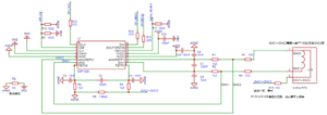
- Circuit connection instructions
- PT100 connection: PT100 (three-wire system) is connected as shown in the schematic.
- Voltage reference generation: The IDAC1 output is connected to AIN2 (internal software configuration required), the IDAC2 output is connected to AIN3 (internal software configuration required), and the two IDAC currents merge at the node and flow together through the external reference resistor Rref(R5). The other end of the REF is connected to the analog ground AVSS. The SSP1220’s positive reference input, REFP0, connects to the upper end of RREF (R5) (the IDAC merge point). The SSP1220’s negative reference input, REFN0, connects to AVSS. Therefore, the reference voltage, VREF= (IIDAC1 + IIDAC2) * RREF.
- Signal measurement: AIN1 for SSP1220 is configured as a differential positive input AINP and SSP1220’s AIN0 is configured as a differential negative input AINN, so that the measured voltage is the potential difference between AIN1 and AIN0.
- Filtering circuitry: RC low-pass filters need to be added on both the analog inputs (AIN0, AIN1, AIN2) and reference inputs (REFP0) for antialiasing and noise suppression. Input filters: consisting of R1, R2, C1 and C6, C5. Reference filter: consists of R3, R4, C2 and C3, C4. To maintain the accuracy of scale measurements, the reference filter’s cut-off frequency should match the input filter.
Ⅲ、Device selection and parameter calculation
The hypothetical design objectives are as follows: PT100 type: three-wire; Temperature measurement range: -200°C ~ +850°C; Supply voltage AVDD: 3.3V (AVSS = 0V); DAC Current: 500μA (per channel); Data rate: 20 SPS (for optimal noise performance).
- Reference resistance (Rref) selection and calculation
Rref is at the heart of the accuracy of the entire system. Function: Generate the reference voltage V ref of the ADC, and its accuracy and stability directly determine the measurement results.
Resistance Calculation:
To maximize the range of the ADC and meet the common mode voltage requirements of the PGA, the Vref is typically set at about half the supply voltage. In this design, AVDD = 3.3V and the target VREF is about 1.65V.
IIDAC = I_IDAC1 + I_IDAC2 = 500uA + 500uA = 1mA
RREF = VREF /(IIDAC1 + IIDAC2) = 1.65V/1mA = 1.65kΩ
A resistor with a nominal value of 1.65 kΩ can be selected. If not found, 1.62kΩ or 1.69kΩ is also an acceptable approximation.
Selection requirements:
Accuracy: At least ±0.1%, recommended ±0.05% or higher for high-precision applications.
Temperature Bleating: Must be very low, with precision film resistance of ±5 ppm/°C or ±10 ppm/°C recommended.
Long-term stability: high.
Never use a normal 1%, 100ppm/°C chip resistor.
- IDAC current and PGA gain options
IDAC Current: 500μA selected. This value strikes a good balance between power consumption, self-heating effect, and signal amplitude. If the current is too small, the signal is weak and easily affected by noise; Too much current may cause the PT100 to self-heat or exceed IDAC compliant voltages.
PGA Gain Selection: The PT100 has a smaller voltage (e.g. 500μA × 100Ω = 50mV), but uses a ratio measurement (the reference voltage is also from IDAC), so there is no need to amplify to avoid saturation, and the gain selection is 1X.
- Filter circuit component selection
Filter Resistors (R1, R2, R3, R4): 1kΩ is usually selected. This value is large enough to effectively filter and small enough to avoid significant offset voltages at the input (due to input bias current). They also act as current-limiting protection.
Differential filter capacitors (C1, C2): Set the cut-off frequency together with the resistor. For example, for a data rate of 20SPS, the cut-off frequency can be set in the tens of Hz. fc = 1 / (2π * (R1+R2) * C1)。 If R1+R2=2kΩ and expects fc ≈ 16Hz, C1 ≈ 1 / (2* 2000 * 16) ≈ 4.7μF. In real-world applications, 100nF (0.1μF) is often used to obtain a wider noise rejection bandwidth. Type: C0G (NPO) ceramic capacitors are recommended for their stable dielectric constant, low voltage coefficient, and low microacoustic effect.
Common-mode filtered capacitors (C5, C6, C3, C4): Typically chosen an order of magnitude smaller than differential capacitors, such as 10nF, to ensure that mismatches of differential capacitors do not result in excessive common-mode noise being converted into differential noise.
Ⅳ、Software configuration
- Master Logic:
float SSP1x20_read_temperature(void)
{
uint32_t ADC_data;
uint32_t ADC_temp1;
//SSP1x20_read_register(SSP1x20_REG0, 4, &Read_REGTab[0]);
Write_REGTab[0] = SSP1x20_MUX_AIN0_AIN1 | SSP1x20_GAIN_1 | SSP1x20_PGA_BYPASS_ON;
Write_REGTab[1]=SSP1x20_DR_20SPS|SSP1x20_MODE_NORMAL|SSP1x20_SC|SSP1x20_TS_ON| SSP1x20_BCS_OFF;
Write_REGTab[2]=SSP1x20_VREF_2048|SSP1x20_REJECT_OFF|SSP1x20_PSW_OFF | SSP1x20_IDAC_1000uA;
Write_REGTab[3] = SSP1x20_IDAC1_AIN2 | SSP1x20_IDAC2_AIN3 | SSP1x20_DRDYM_DRDY;
SSP1x20_WriteRegister(SSP1x20_REG0, 4, &Write_REGTab[0]);
SSP1x20_SendCommand(SSP1x20_CMD_START);
SPI_ADC_CS_LOW();
while (ADC_DRDY_GAIN == 1);//SSP1x20_DRDYM_DRDY
- The main configuration and description of the program
- Configure register 0: MUX and gain
Write_REGTab[0] = SSP1x20_MUX_AIN0_AIN1 | SSP1x20_GAIN_1 | SSP1x20_PGA_BYPASS_ON;
| Bit | Configuration | Function | Description |
| BIT7~BIT4 | MUX_AIN0_AIN1 | Differential input channel selection | AIN0 – AIN1 → for PT100 voltage measurement |
| BIT3~BIT1 | GAIN_1(1x gain ) | Gain settings | 1× (no need to amplify as Vin ≈ 1V) |
| BIT0 | PGA_BYPASS_ON | PGA bypass | Switch off the programmable gain amplifier to prevent signal distortion |
- Configuration register 1: Sample rate and mode
Write_REGTab[1] = SSP1x20_DR_20SPS | SSP1x20_MODE_NORMAL | SSP1x20_SC | SSP1x20_TS_OFF | SSP1x20_BCS_OFF;
| Bit | Configuration | Function | Description |
| BIT7~BIT5 | DR_20SPS | Data rate | 20 times/sec → suitable for slow temperature changes |
| BIT4~BIT3 | MODE_NORMAL | Normal working mode | Not single or consecutive |
| BITO | SC | Self-calibration enabled | Improved accuracy (recommended on) |
| BIT1 | TS_OFF | Disable the internal temperature sensor | TS_ON turn on the internal temperature sensor, the configuration for measuring the external temperature does not work (this configuration has the highest priority) |
- Configure register 2: Reference voltage with IDAC
Write_REGTab[2] = SSP1x20_VREF_2048 | SSP1x20_REJECT_OFF | SSP1x20_PSW_OFF | SSP1x20_IDAC_500uA;
| Bit | Configuration | Function | Description |
| BIT7~BIT6 | VREF_2048 | External reference voltage | Use an external R_REFR_REF to generate a reference voltage (e.g., 1.65kΩ). |
| BIT5~BIT4 | REJECT_OFF | No notch filtering | No power frequency interference immunity is required |
| BIT3 | PSW_OFF | Do not enable the power switch | Maintain normal power supply |
| BIT2~BIT0 | IDAC_500uA | Excitation current | Set to 500 μA to avoid 3.9kΩ × 1mA = 3.9V > 3.3V overvoltage |
| Bit | Configuration | Function | Description |
| BIT7~BIT5 | IDAC1_AIN2 | IDAC1 output to AIN2 | The excitation current flows through the top end of the PT100 |
| BIT4~BIT2 | IDAC2_AIN3 | IDAC2 output to AIN3 | Return to the path to cancel out the lead resistance |
| BIT1 | DRDYM_DRDY | DRDY mode | Use the DRDY signal to notify you that the conversion is complete |
(4) Configure register 3: IDAC route channel with DRDY
- Three-wire PT100 core:
Current Path:
- IDAC1 → AIN2 → PT100 → AIN1
- IDAC2 → AIN3 → AIN1(Return)
- Two currents are equal → offset the voltage drop on the R_LEAD2R_LEAD2
uint32_t raw_u24 = SSP1x20_read_data_drdy();
SSP1220 outputs 24-bit data, but MCUs typically read in 32-bit (SPI reads 4 bytes at a time).
if (raw < 0) raw = -raw;
The PT100 voltage is always positive (current flows from AIN0 to AIN1).
If raw < 0, the AIN0 and AIN1 software configurations are reversed.
printf(“Raw: %ld, R=%.3f Ω, Temp=%.2f °C\r\n”, raw, R_pt100, temperature);
Print the original code value, calculate the resistance, and the final temperature for easy debugging
If Raw is negative→ the configuration is reversed
If R > 1400Ω → indicates that the IDAC or Rref is set incorrectly
If Temp = -999 → indicates that the R-value is outside the reasonable range
Ⅴ、Measurement procedure and results
- PT100 voltage measurement program at both ends:
void SSP1x20_ADC_MeasurePt100(void)
{
float V_ref = 2.048; // Internal reference voltage 2.048V
//printf(“\r\n Multi-point single voltage measurement \r\n”);
Write_REGTab[0] = SSP1x20_MUX_AIN1_AIN0 | SSP1x20_GAIN_1 | SSP1x20_PGA_BYPASS_OFF;
Write_REGTab[1] = SSP1x20_DR_20SPS | SSP1x20_MODE_NORMAL | SSP1x20_SC | SSP1x20_TS_OFF | SSP1x20_BCS_OFF;
Write_REGTab[2] = SSP1x20_VREF_REF0 | SSP1x20_REJECT_OFF | SSP1x20_PSW_OFF | SSP1x20_IDAC_500uA;
Write_REGTab[3] = SSP1x20_IDAC1_AIN2 | SSP1x20_IDAC2_AIN3 | SSP1x20_DRDYM_DRDY;
SSP1x20_WriteRegister(SSP1x20_REG0, 4, &Write_REGTab[0]);
printf(“Write_REGTab[0]=%x\r\n”, Write_REGTab[0]);
printf(“Write_REGTab[1]=%x\r\n”, Write_REGTab[1]);
printf(“Write_REGTab[2]=%x\r\n”, Write_REGTab[2]);
printf(“Write_REGTab[3]=%x\r\n”, Write_REGTab[3]);
while (1)
{
SSP1x20_SendCommand(SSP1x20_CMD_START); // When continuous measurement is enabled, this command is sent only once
HAL_Delay(100);
SPI_ADC_CS_LOW();
}
SSP1220 test results
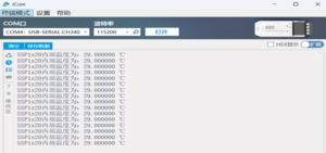
- SSP1220 internal temperature measurement
Internal temperature test function
float SSP1x20_read_temperature(void)
{
uint32_t ADC_data;
uint32_t ADC_temp1;
//SSP1x20_read_register(SSP1x20_REG0, 4, &Read_REGTab[0]);
Write_REGTab[0] = SSP1x20_MUX_AIN0_AIN1 | SSP1x20_GAIN_1 | SSP1x20_PGA_BYPASS_ON;
Write_REGTab[1] = SSP1x20_DR_20SPS | SSP1x20_MODE_NORMAL | SSP1x20_SC | SSP1x20_TS_ON | SSP1x20_BCS_OFF;
Write_REGTab[2] = SSP1x20_VREF_2048 | SSP1x20_REJECT_OFF | SSP1x20_PSW_OFF | SSP1x20_IDAC_1000uA;
Write_REGTab[3] = SSP1x20_IDAC1_AIN2 | SSP1x20_IDAC2_AIN3 | SSP1x20_DRDYM_DRDY;
SSP1x20_WriteRegister(SSP1x20_REG0, 4, &Write_REGTab[0]);
SSP1x20_SendCommand(SSP1x20_CMD_START);
SPI_ADC_CS_LOW();
while (ADC_DRDY_GAIN == 1);//SSP1x20_DRDYM_DRDY
Internal temperature test configuration details:
Write_REGTab[1] = SSP1x20_DR_20SPS | SSP1x20_MODE_NORMAL | SSP1x20_SC | SSP1x20_TS_ON | SSP1x20_BCS_OFF;
- SSP1x20_TS_ON: Enable the internal temperature sensor (critical), this configuration has the highest priority
- SSP1x20_SC: Perform self-calibration (recommended)
- 20SPS: Low speed and high accuracy, suitable for temperature measurement
Write_REGTab[2] = SSP1x20_VREF_2048 | SSP1x20_REJECT_OFF | SSP1x20_PSW_OFF | SSP1x20_IDAC_1000uA;
- SSP1x20_VREF_2048: Use an internal 2.048V reference voltage (not external REF0!) )
- Because the internal temperature sensor is an absolute voltage output, a fixed reference voltage must be used to convert the temperature.
- IDAC_1000uA: Although IDAC is enabled, IDAC in TS_ON mode does not affect internal temperature measurements (negligible).
Write_REGTab[3] = SSP1x20_IDAC1_AIN2 | SSP1x20_IDAC2_AIN3 | SSP1x20_DRDYM_DRDY;
- Configure the IDAC pin and DRDY, but have no effect on the internal temperature measurement (just keep the registers intact).
- 2 Start the conversion and wait for DRDY
SSP1x20_SendCommand(SSP1x20_CMD_START); SPI_ADC_CS_LOW();while (ADC_DRDY_GAIN == 1); // 等待 DRDY 变低
- Send the START command to start a continuous transition
- Wait for the DRDY pin to go low, indicating that the data is ready
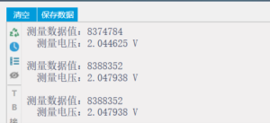
The measurement of indoor room temperature is shown in the figure below:
3. External temperature measurement (method 1, simplified factor 0.385 calculation)
External temperature test related code:
uint32_t ADC_gain_value = 0; // Readout data
uint32_t ADC_value = 0; // Measure the data value
float tmpPt100=0;
float RTD=0;
void SSP1x20_ADC_Measure(void)
{
printf(“\r\n Multi-point single voltage measurement \r\n”);
Write_REGTab[0] = SSP1x20_MUX_AIN1_AIN0 | SSP1x20_GAIN_1 | SSP1x20_PGA_BYPASS_OFF; SSP1x20_MUX_AIN1_AIN0 Interface AIN1 AIN0 should be selected based on the actual circuit diagram
Write_REGTab[1] = SSP1x20_DR_20SPS | SSP1x20_MODE_NORMAL | SSP1x20_SC | SSP1x20_TS_OFF | SSP1x20_BCS_OFF;
Write_REGTab[2] = SSP1x20_VREF_REF0 | SSP1x20_REJECT_OFF | SSP1x20_PSW_OFF | SSP1x20_IDAC_500uA;
Write_REGTab[3] = SSP1x20_IDAC1_AIN2 | SSP1x20_IDAC2_AIN3 | SSP1x20_DRDYM_DRDY;
SSP1x20_WriteRegister(SSP1x20_REG0, 4, &Write_REGTab[0]);
printf(“Write_REGTab[0]=%x\r\n”, Write_REGTab[0]);
printf(“Write_REGTab[1]=%x\r\n”, Write_REGTab[1]);
printf(“Write_REGTab[2]=%x\r\n”, Write_REGTab[2]);
printf(“Write_REGTab[3]=%x\r\n”, Write_REGTab[3]);
while (1)
{
SSP1x20_SendCommand(SSP1x20_CMD_START); When continuous measurement is enabled, this command is sent only once
HAL_Delay(100);
SPI_ADC_CS_LOW();
ADC_gain_value =0;
ADC_gain_value = SPI_ADC_ReadByte();
ADC_gain_value = (ADC_gain_value << 8) | SPI_ADC_ReadByte();
ADC_gain_value = (ADC_gain_value << 8) | SPI_ADC_ReadByte();
SPI_ADC_CS_HIGH();
RTD = 1650*( (float)ADC_gain_value /(0x3fffff));//Reference resistance 1650 ohms
tmpPt100 = (RTD-100)/0.38;
__NOP();
printf(“R=%.3f Ω, Temp=%.2f °C\r\n”,RTD, tmpPt100 );
}
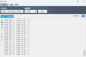
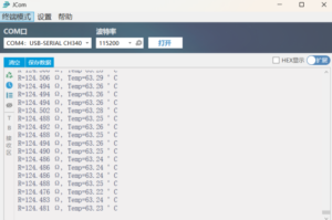
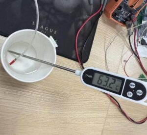
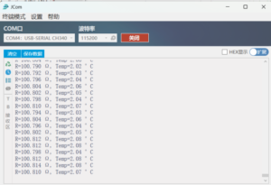
The results of the three-line RTD measurement of the temperature of the ice water mixture are shown in the figure below:

External temperature measurements (method two, calculated by the Callendar-Van Dusen equation) are more accurate
Master Code:
//High accuracy RTD -> temperature
static float rtd_to_temperature_iec60751(float rtd)
{
if (rtd < 0.0f) return -999.0f; // illegal value
float t = (rtd – R0_PT100) / 0.385f; // initial guess
if (rtd <= R0_PT100) {
//T < = 0°C: Use the complete equation
for (int i = 0; i < 10; i++) {
float rt_calc = R0_PT100 * (1.0f + A_COEFF*t + B_COEFF*t*t + C_COEFF*(t – 100.0f)*t*t*t);
float dr_dt = R0_PT100 * (A_COEFF + 2.0f*B_COEFF*t + C_COEFF*(4.0f*t*t*t – 300.0f*t*t));
float error = rt_calc – rtd;
t -= error / dr_dt;
if (fabsf(error) < 0.001f) break;
}
} else {
// T >= 0°C:: Use the simplified equation
for (int i = 0; i < 10; i++) {
float rt_calc = R0_PT100 * (1.0f + A_COEFF*t + B_COEFF*t*t);
float dr_dt = R0_PT100 * (A_COEFF + 2.0f*B_COEFF*t);
float error = rt_calc – rtd;
t -= error / dr_dt;
if (fabsf(error) < 0.001f) break;
}
}
return t;
}
/**
* @brief Analog channel ADC measurement (external temperature measurement)
* @param None
* @retval None
*/
uint32_t ADC_gain_value = 0; // Readout data
uint32_t ADC_value = 0; // Measure the data value
float tmpPt100=0;
float RTD=0;
void SSP1x20_ADC_Measure(void)
{
printf(“\r\n Multi-point single voltage measurement \r\n”);
Write_REGTab[0] = SSP1x20_MUX_AIN1_AIN0 | SSP1x20_GAIN_1 | SSP1x20_PGA_BYPASS_OFF;
Write_REGTab[1] = SSP1x20_DR_20SPS | SSP1x20_MODE_NORMAL | SSP1x20_SC | SSP1x20_TS_OFF | SSP1x20_BCS_OFF;
Write_REGTab[2] = SSP1x20_VREF_REF0 | SSP1x20_REJECT_OFF | SSP1x20_PSW_OFF | SSP1x20_IDAC_500uA;
Write_REGTab[3] = SSP1x20_IDAC1_AIN2 | SSP1x20_IDAC2_AIN3 | SSP1x20_DRDYM_DRDY;
// Write_REGTab[3] = SSP1x20_IDAC1_AIN3 | SSP1x20_IDAC2_AIN2 | SSP1x20_DRDYM_DRDY;
SSP1x20_WriteRegister(SSP1x20_REG0, 4, &Write_REGTab[0]);
printf(“Write_REGTab[0]=%x\r\n”, Write_REGTab[0]);
printf(“Write_REGTab[1]=%x\r\n”, Write_REGTab[1]);
printf(“Write_REGTab[2]=%x\r\n”, Write_REGTab[2]);
printf(“Write_REGTab[3]=%x\r\n”, Write_REGTab[3]);
while (1)
{
SSP1x20_SendCommand(SSP1x20_CMD_START); When continuous measurement is enabled, this command is sent only once
HAL_Delay(100);
SPI_ADC_CS_LOW();
ADC_gain_value =0;
ADC_gain_value = SPI_ADC_ReadByte();
ADC_gain_value = (ADC_gain_value << 8) | SPI_ADC_ReadByte();
ADC_gain_value = (ADC_gain_value << 8) | SPI_ADC_ReadByte();
SPI_ADC_CS_HIGH();
#define CALIBRATED_FULL_SCALE 4210300.0f // ccording to calibration data
RTD = 1650.0f * ((float)ADC_gain_value / CALIBRATED_FULL_SCALE);
tmpPt100 = rtd_to_temperature_iec60751(RTD);
__NOP();
printf(“R=%.3f Ω, Temp=%.2f °C\r\n”,RTD, tmpPt100 );
}
}
The test results are shown in the figure:
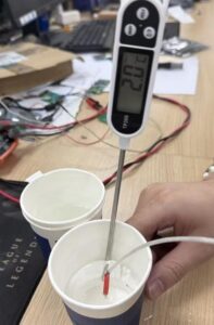
Hot Water Temperature Test:
Ice Water Mixture Test:
4. External temperature test configuration details:
| Register | Configure values (your code) | Function description: | Why did you choose this? |
| REG0 Write_REGTab[0] | SSP1x20_MUX_AIN1_AIN0 | SSP1x20_GAIN_1 |SSP1x20_PGA_BYPASS_OFF | Enter Channel Selection + Gain Settings | |
| SSP1x20_MUX_AIN1_AIN0 | Differential inputs: AIN1 is positive and AIN0 is negative | The PT100 is connected to AIN0 and AIN1 on both ends and requires differential voltage measurement. ⚠️ Note the polarity: if the configuration is reversed, the ADC outputs a negative value (e.g., 0x800000), resulting in a negative temperature. | |
| SSP1x20_GAIN_1 | Gain = 1 | The PT100 has a smaller voltage (e.g. 500μA × 100Ω = 50mV), but uses a ratio measurement (the reference voltage is also from IDAC), so no amplification is required to avoid saturation. | |
| SSP1x20_PGA_BYPASS_OFF | No bypass PGA | Keep the PGA function (even if the gain=1) to ensure the signal path is normal. | |
| REG1 Write_REGTab[1] | SSP1x20_DR_20SPS | SSP1x20_MODE_NORMAL | SSP1x20_SC | SSP1x20_TS_OFF | SSP1x20_BCS_OFF | Data rate + operating mode | |
| SSP1x20_DR_20SPS | Sample rate = 20 sample points/second | Low speed improves accuracy, suppresses noise, and is suitable for temperature measurement (slow change). | |
| SSP1x20_MODE_NORMAL | Normal continuous conversion mode | Continuous data output for real-time monitoring. | |
| SSP1x20_SC | Perform self-calibration | Calibration after each configuration, eliminates offset/gain errors and improves accuracy. | |
| SSP1x20_TS_OFF | Turn off the internal temperature sensor | We measure the external PT100 and do not need the internal temperature. | |
| SSP1x20_BCS_OFF | Disable burn-off current sources | No, you don’t. | |
| REG2 Write_REGTab[2] | SSP1x20_VREF_REF0 | SSP1x20_REJECT_OFF | SSP1x20_PSW_OFF SSP1x20_IDAC_500uA | Reference Voltage + IDAC Settings | |
| SSP1x20_VREF_REF0 | Use an external reference voltage (REF0 = voltage between AIN2/AIN3). | Implement ratio-based measurements: ADC result = (Vpt100 / Vref) × 224, independent of IDAC current absolute, only related to Rref, resistant to power supply fluctuations. | |
| SSP1x20_REJECT_OFF | 50/60Hz suppression is not enabled | If the environmental interference is small, it can be turned off; If it is in a power frequency environment, it is recommended to turn on the REJECT_50. | |
| SSP1x20_PSW_OFF | Turn off the sensor power supply switch | The PT100 is powered by IDAC and does not require additional PSW. | |
| SSP1x20_IDAC_500uA | Set constant current source current = 500 μA | Common current values, balancing power consumption and signal amplitude (100Ω → 50mV). | |
| REG3 Write_REGTab[3] | SSP1x20_IDAC1_AIN2 | SSP1x20_IDAC2_AIN3 | SSP1x20_DRDYM_DRDY | IDAC output pin + DRDY configuration | |
| SSP1x20_IDAC1_AIN2 | IDAC1 output to AIN2 | AIN2 to PT100 (excitation) | |
| SSP1x20_IDAC2_AIN3 | IDAC2 output to AIN3 | AIN3 is connected to the reference resistor at one end of the R_ref (forming the loop) → realizes three-wire compensation (offsetting the wire resistance). | |
| SSP1x20_DRDYM_DRDY | Enable the DRDY pin (Data Ready Signal). | The MCU detects DRDY low levels through GPIO to know when data is being read and avoid polling. |
——————————————————————————————————
Key Part Code Formula Calculation:
RTD = 1650*( (float)ADC_gain_value /(0x3fffff)); //reference resistance 1650 ohms tmpPt100 = (RTD-100)/0.385;
Reference resistance 1650 ohms,
First line code RTD = 1650 * (ADC / 0x3FFFFF)
Designed to convert the original ADC value to the resistance value of the PT100 (ratio measurement)
- VIN = I × RPT100 (voltage across PT100)
- VREF = I × RREF (voltage across reference resistor)
The same constant current source I adc is used at both ends
So: Vin/Vref = Rpt100/Rref
The output of the ADC is the digitized result of this ratio
ADC_Code = Vin/Vref x 224
So pushed back
Rpt100= Rref x ADC_Code /224
———————————————————————————————————————
Second line code: tmpPt100 = (RTD – 100) / 0.385;
Estimate the temperature with a linear approximation formula
At 0°C, Rpt100 = 100 Ω
For every 1°C increase in temperature, the resistance increases by about 0.385 Ω
So
T ≈ (R-100)/0.385
Ⅵ、 Common Problem Debugging Guide
| Anomal | Possible causes | Troubleshooting steps |
| The original value of the ADC (raw) is negative | AIN0 is the opposite of AIN1 configuration | 1. Check that the software configuration is consistent with the connection to the hardware |
| R_PT100 > 1400Ω | 1. Incorrect IDAC current configuration; 2. Rref opens | 1. Check the IDAC configuration of REG2 (make sure it is 500μA); 2. Measure the R ref resistance value with a multimeter to confirm that the circuit is not open |
| The temperature value is – 999°C | PT100 exceeds the 18Ω~330Ω range | 1. Check if the PT100 is disconnected (measure the PT100 resistance); 2. Verify SPI Communication (Read Register Configuration Values) |
| Temperature fluctuations > 0.1°C | 1. Large ripple of power supply; 2. Electromagnetic interference | 1. Measure SSP1220 VDD ripple (≤ 10mV required); 2. Check the grounding of the shield wire to avoid interference |
Ⅶ、 SSP1220 Core register configuration table
| Register | Configure items | Value (external temperature measurement) | Function description: |
| REG0 | Differential channels | AIN1-AIN0 | Match the PT100 wiring to avoid negative raw |
| gain | 1× | Avoid signal saturation and adapt to ratio measurement | |
| PGA bypass | disable | Preserve signal path integrity | |
| REG1 | Sampling rate | 20SPS | Low speed improves accuracy and adapts to slow temperature signals |
| Working mode | Normal mode | Continuous conversion and real-time output of temperature data | |
| Self-calibration | enable | Eliminate offset/gain errors and improve accuracy | |
| Internal TS | disable | External temperature measurement does not require internal sensors | |
| REG2 | Reference voltage | External REF0 | Ratio-based measurement to counteract IDAC current fluctuations |
| IDAC current | 500μA | Balanced Power Consumption and Signal Amplitude (50mV 100Ω) | |
| REG3 | IDAC1 routes | AIN2 | The excitation current input PT100 |
| IDAC2 routes | AIN3 | Counteract the lead resistor R7 |
Ⅷ、Callendar-Van Dusen equation coefficient table
| Coefficient | Numeric value | Unit | Scope of application |
| R0 | 100.0 | Ω | 0°C reference resistance |
| A | 3.9083×10⁻³ | ℃-1 | -200℃~600℃ |
| B | -5.775×10⁻⁷ | ℃-2 | -200℃~600℃ |
| C | -4.183×10⁻¹² | ℃-4 | -200℃~0℃ |
The full code can be obtained by contacting our technical support. Contact: 18014203727

