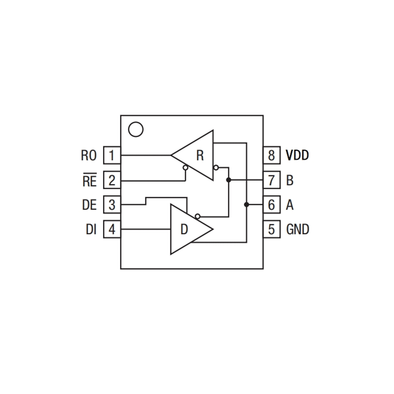
Features
Other pins have level 3 ESD protection:>+8kV HBM
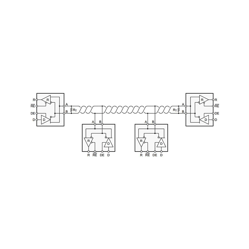
| Applications
|
_画板-1@2x.png)


Absolute Maximum Ratings
Unless specified otherwise, Tamb= 25℃
| Parameter | Symbol | Value | Unit |
| Supply Voltage | VDD | -0.3~7 | V |
| Input / Output Voltage | VIN/VOUT | GND-0.3~VDD+0.3 | V |
| A/B Input / Output Voltage | VINA/B/VOUTA/B | -13~13 | V |
| Operating Temperature | Tamb | -40~85 | ℃ |
| Storage Temperature | T | -65~150 | ℃ |
Electrical Characteristics
DC Electrical Characteristics
Unless specified otherwise,VDD=5V±5%,Tamb= 25℃
| Parameter | Symbol | Test Conditions | Min | Typ | Max | Unit | ||
| Driver | ||||||||
| Differential driver output | VOD1 | No load | VDD | V | ||||
| Differential driver output | VOD2 | R=50Ω(RS-422)(1) | 2.0 | V | ||||
| R=27Ω(RS-485)(1) | 1.8 | V | ||||||
| Change in magnitude of driver differential output voltage for complementary output states | ΔVOD | R=50Ω or 27Ω(1) | 0.2 | V | ||||
| Driver common-mode output voltage | VOC | R=50Ω or 27Ω(1) | 3 | V | ||||
| Change in magnitude of driver common-mode output voltage for complementary output states | ΔVOC | R=50Ω or 27Ω(1) | 0.2 | V | ||||
| Input high voltage | VIH1 | DE、 | 2.0 | V | ||||
| Input low voltage | VIL1 | DE、 | 0.8 | V | ||||
| Input current | IIN1 | DE、 | -2 | 2 | mA | |||
| DI Input hysteresis voltage | Vhys | 100 | mA | |||||
| Input current (A, B) | IIN2 | DE=GND,VDD =GND or 5.25V | Vin=12V | 150 | mA | |||
| Vin=-7V | -150 | mA | ||||||
| Driver short-circuit current | IOD1 | -7V≤VOUT≤VDD | -100 | mA | ||||
| 0V≤VOUT≤12V | 100 | mA | ||||||
| 0V≤VOUT≤VDD | ±25 | mA | ||||||
| Receiver | ||||||||
| Differential threshold voltage | VTH | -7V≤VCM≤12V | -200 | -125 | -50 | mV | ||
| input hysteresis voltage | ΔVTH | 40 | mV | |||||
| output high voltage | VOH | IO=-4mA,VID=-50mV | VDD-1 | V | ||||
| output low voltage | VOL | IO=4mA,VID=-200mV | 0.4 | V | ||||
| 3-state(high impedance) output current at receiver | IOZR | 0.4V≤VO≤2.4V | ±1 | mA | ||||
| input resistance | RIN | -7V≤VCM≤12V | 96 | kΩ | ||||
| Receiver short-circuit current | IOSR | 0V≤VRO≤VDD | ±7 | ±100 | mA | |||
| Supply Current | ICC | No load, | DE=VDD | 450 | 1100 | mA | ||
| DE=GND | 450 | 1000 | mA | |||||
| Supply Current in Shutdown | ISHDN | DE=GND, | 10 | mA | ||||
| ESD Protection(A/B) | ESD | Human Body Model | ±15 | kV | ||||
Transmission characteristics
Unless specified otherwise,VDD=5V±5%,Tamb= 25℃
| Parameter | Symbol | Test Conditions | Min. | Typ. | Max. | Unit |
| slew-rate-limited | ||||||
| Driver Input to Output | tDPLH | RDIFF=54Ω,CL1=CL2=100pF(2) | 30 | 60 | ns | |
| Driver Input to Output | tDPHL | RDIFF=54Ω,CL1=CL2=100pF(2) | 30 | 60 | ns | |
| |tDPLH-tDPHL| | tDSKEW | RDIFF=54Ω,CL1=CL2=100pF(2) | 20 | ns | ||
| Driver Rise or Fall Time | tDR,tDF | RDIFF=54Ω,CL1=CL2=100pF(2) | 30 | ns | ||
| Maximum Data Rate | fMAX | 10 | Mbps | |||
| Driver Enable to Output High | tDZH | CL=100pF,S2 closed(3) | 70 | ns | ||
| Driver Enable to Output Low | tDZL | CL=100pF,S1 closed(3) | 70 | ns | ||
| Driver Disable Time from Low | tDLZ | CL=15pF,S1 closed(3) | 70 | ns | ||
| Driver Disable Time from Low | tDHZ | CL=15pF,S2 closed(3) | 70 | ns | ||
| Receiver Input to Output | tRPLH | |VID|≥2.0V Rise or Fall Time≤15ns(4) | 90 | 250 | ns | |
| Receiver Input to Output | tRPHL | 90 | 250 | ns | ||
| |tRPLH-tRPHL| | tRSKD | |VID|≥2.0V Rise or Fall Time≤15ns(4) | 30 | ns | ||
| Receiver Enable to Output Low | tRZL | CL=100pF,S1 closed(5) | 30 | 70 | ns | |
| Receiver Enable to Output High | tRZH | CL=100pF,S2 closed(5) | 30 | 70 | ns | |
| Receiver Disable Time from Low | tRLZ | CL=100pF,S1 closed(5) | 30 | 70 | ns | |
| Receiver Disable Time from High | tRHZ | CL=100pF,S2 closed(5) | 30 | 70 | ns | |
| Time to Shutdown | tSHDN | 200 | 600 | ns | ||
Note:
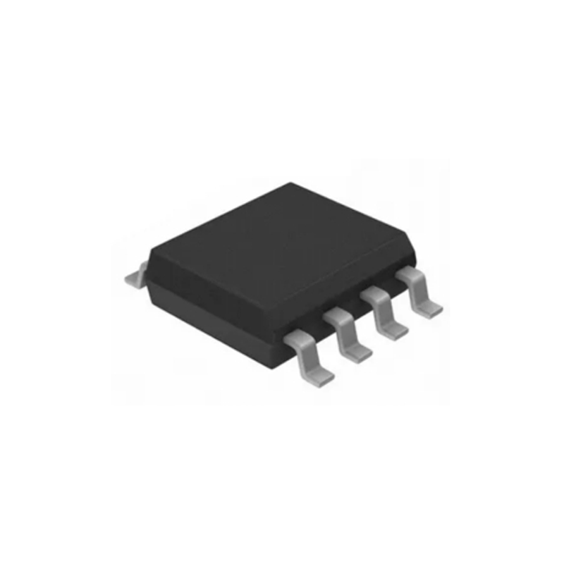
Order specification
| Part No | Package | Manner of Packing | Devices per bag/reel |
| SSP3485 | SOP8 | Reel | 3500 |
| SSP3485U | MSOP8 | Reel | 5000 |