

Features
| Applications
|
Blog
Features
| Applications
|
Absolute Maximum Ratings
| Parameter | Rating |
| VDD to AGND | −0.3 V to +7 V |
| VDD to DGND | −0.3 V to +7 V |
| Analog Input Voltage to AGND (VAP, VBP, VCP, VN, IAP, IAN, IBP, IBN, ICP, and ICN) | −6 V to +6 V |
| Reference Input Voltage to AGND | −0.3 V to V + 0.3 V DD |
| Digital Input Voltage to DGND | −0.3 V to V + 0.3 V DD |
| Digital Output Voltage to DGND | −0.3 V to V + 0.3 V DD |
| Operating Temperature Range Industrial | −40°C to +85°C |
| Storage Temperature Range | −40°C to +85°C |
| Junction Temperature | 150°C |
| 24-Lead SOIC, Power Dissipation | 450 mW |
| θJA Thermal Impedance | 250°C/W |
| Lead Temperature, Soldering | |
| Vapor Phase (60 sec) | 215°C |
| Infrared (15 sec) | 220°C |
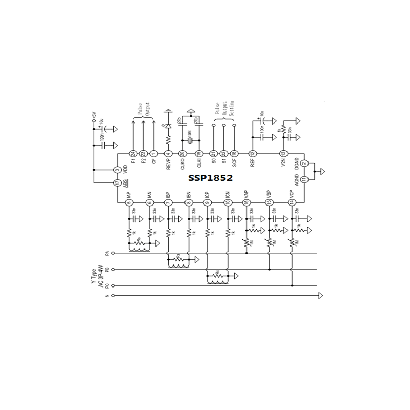
Electrical Characteristics
(VDD = 5 V ± 5%, AGND = DGND = 0 V, on-chip reference, CLKIN = 10 MHz, TMIN to TMAX = –40°C to +85°C, unless otherwise noted.)
| Parameter | Value | Unit | Conditions |
| ACCURACY | |||
| Measurement Error on Current Channel | 0.1 | %Reading typ | Voltage channel with full-scale signal (±500 mV), 25°C, over a dynamic range of 500 to 1 |
| Phase Error Between Channels PF = 0.8Capacitive | ±0.1 | Degrees | Line frequency 50~60Hz |
| Phase Error Between Channels PF = 0.5Inductive | ±0.1 | Degrees | |
| AC Power Supply Rejection Output Frequency Variation(CF) | 0.2 | %Reading typ | SCF=0,S1=S0=1, IA=IB=IC=100mVrms,50Hz VA=VB=VC=100mVrms,50Hz ripple on VDD of 175 mV rms,100Hz |
| DC Power Supply Rejection Output Frequency Variation(CF) | ±0.3 | %Reading typ | S1=1,S0=SCF=0 IA=IB=IC=100mV rms,50Hz VA=VB=VC=100mVrms,50Hz VDD =5V±250mV |
| ANALOG INPUTS | |||
| Maximum Signal Levels | ±0.5 | Vmax | VA,VB,VC,IA,IB,IC to GND |
| Input Impedance (DC) | 390 | kΩ min | CLKOSC=10MHz |
| Bandwidth(-3dB) | 14 | kHz typ | CLKOSC/256,CLKOSC=10MHz |
| ADC Offset Error | ±16 | mV max | |
| Gain Error | ±9 | %Ideal typ | External 2.5V reference IAP=IBP=ICP=500mV ,dc |
| ON-CHIP REFERENCE | |||
| Reference Error | ±200 | mV max | Nominal 2.5V |
| Temperature Coefficient | 30 | ppm/℃ typ | |
| CLKIN | |||
| Input Clock Frequency | 12 | MHz max | All specifications for CLKIN of 10 MHz |
| 8 | MHz min | ||
| LOGIC INPUTS SCF, S0, S1 and ABS | |||
| Input High Voltage, VINH | 2.4 | V min | VDD=5V±5% |
| Input Low Voltage, VINL | 0.8 | V max | VDD=5V±5% |
| Input Current, IIN | ±3 | μA max | Typically 10nA,VIN=0V to VDD |
| Input Capacitance, CIN | 10 | pF max | |
| LOGIC OUTPUT F1 and F2 | |||
| Output High Voltage, VOH | 4.5 | V min | ISOURCE=10mA,VDD=5V |
| Output Low Voltage, VOL | 0.5 | V max | ISINK=10mA,VDD=5V |
| CF and REVP | |||
| Output High Voltage, VOH | 4 | V min | ISOURCE=10mA,VDD=5V |
| Output Low Voltage, VOL | 0.5 | V max | ISINK=10mA,VDD=5V |
| POWER SUPPLY For specified performance | |||
| VDD | 4.75 | V min | 5V-5% |
| 5.25 | V max | 5V+5% | |
| IDD | 8 | mA max | |
| 5 | mA min | Typically 6.5mA | |
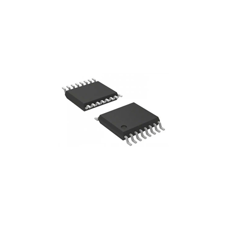
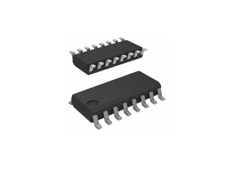
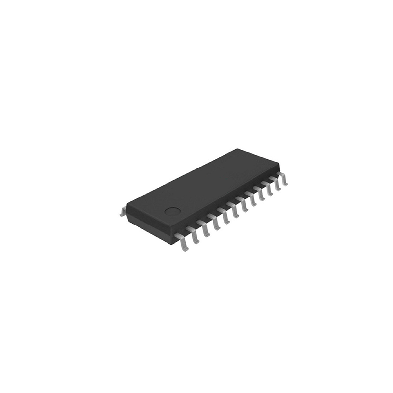
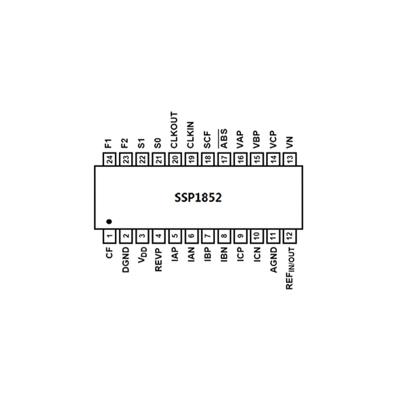
Order Information
| Product model | package | manner of packing | Minimum packing quantity |
| SSP1852 | SOP24 | Tube | 30PCS |

_画板-1@2x.png)
Shanghai Siproin
Microelectronics Co.,Ltd.
Welcome your contact.

