Features
| Application
|
_画板-1@2x.png)


Absolute Maximum Ratings
| Parameter | MIN | MAX | Unit | |
| Power-supply voltage | AVDD to AVSS | -0.3 | 7 | V |
| DVDD to DGND | -0.3 | 7 | V | |
| AVSS to DGND | –2.8 | 0.3 | V | |
| Analog input voltage | AIN0/REFP1, AIN1, AIN2, AIN3/REFN1, REFP0, REFN0 | AVSS-0.3 | AVDD+0.3 | V |
| Digital input voltage | DGND-0.3 | DVDD+0.3 | V | |
| Input current | Continuous, any pin except power supply pins | -10 | 10 | mA |
| Temperature | Junction, TJ | -40 | 150 | ℃ |
| Storage, Tstg | -60 | 150 | ℃ |
Electrical Characteristics
Default Test Condition: Minimum and maximum specifications apply from TA = –40℃ to +125℃. Typical specifications are at TA = 25℃. AVDD=DVDD=3.3V, AVSS=0V, PGA disabled, DR=20SPS, and external Vref=2.048 V(unless otherwise noted).
| Parameter | Symbol | Test Conditions | Min. | Typ. | Max. | Unit |
| SYSTEM PERFORMANCE | ||||||
| Resolution (no missing codes) | 24 | Bits | ||||
| Data rate | DR | Normal mode | 20, 45, 90, 175, 330, 600, 1000 | SPS | ||
| Duty-cycle mode | 5, 11.25, 22.5, 44, 82.5, 150, 250 | SPS | ||||
| Turbo mode | 40, 90, 180, 350, 660, 1200, 2000 | SPS | ||||
| Noise (input-referred) | See the Noise Performance section | |||||
| Integral nonlinearity | INL | Gain=1 to 128, VCM=0.5*AVDD, best fit | 20 | ppmFSR | ||
| Input offset voltage | VIO | PGA disabled, gain = 1 to 4, differential inputs | ±2 | µV | ||
| Gain= 1 to 128, differential inputs | ±2 | µV | ||||
| Offset drift | PGA disabled, gain = 1 to 4 | 0.1 | 0.3 | µV/℃ | ||
| Gain= 1 to 128, TA= –40℃ to +85℃ | 0.1 | 0.3 | µV/℃ | |||
| Gain = 1 to 128 | 0.3 | 0.5 | µV/℃ | |||
| Gain error | PGA disabled, gain = 1 to 4 | 0.2 | % | |||
| Gain = 1 to 128, TA = 25℃ | -0.5 | ±0.2 | 0.5 | % | ||
| Gain drift | PGA disabled, gain = 1 to 4 | 5 | ppm/℃ | |||
| Gain = 1 to 128 | 5 | 20 | ppm/℃ | |||
| Normal-mode rejection ratio | NMRR | 50 Hz ±3%, DR = 20 SPS, external CLK, 50/60 bit = 10 | 105 | dB | ||
| 60 Hz ±3%, DR = 20 SPS, external CLK, 50/60 bit = 11 | 105 | dB | ||||
| 50 Hz or 60 Hz ±3%, DR = 20 SPS, external CLK, 50/60 bit = 01 | 90 | dB | ||||
| Common-mode rejection ratio | CMRR | At dc, gain = 1 | 97 | dB | ||
| f(CM) = 50 Hz, DR = 2000 SPS | 116 | dB | ||||
| f(CM) = 60 Hz, DR = 2000 SPS | 116 | dB | ||||
| Power-supply rejection ratio | PSRR | AVDD at dc, VCM= 0.5AVDD, gain= 1 | 80 | 105 | dB | |
| DVDD at dc, VCM=0.5AVDD, gain=1 | 100 | 115 | dB | |||
| INTERNAL VOLTAGE REFERENCE | ||||||
| Initial accuracy | TA = 25℃ | 2.048 | V | |||
| Reference drift | -45~125℃ | 5 | 30 | ppm/℃ | ||
| -45~85℃ | 4 | 10 | ppm/℃ | |||
| 0~85℃ | 3 | 7 | ppm/℃ | |||
| VOLTAGE REFERENCE INPUTS | ||||||
| Reference input current | REFP0 = Vref, REFN0 = AVSS | 180 | nA | |||
| INTERNAL OSCILLATOR | ||||||
| Internal oscillator accuracy | Normal mode | -2 | ±1 | 2 | % | |
| EXCITATION CURRENT SOURCES (IDACs) | ||||||
| Current settings | 50, 100, 250, 500, 1000, 1500 | µA | ||||
| Compliance voltage | All current settings | AVDD–0.9 | V | |||
| Accuracy | All current settings, each IDAC | -6 | ±1 | 6 | % | |
| EXCITATION CURRENT SOURCES (IDACs) | ||||||
| Current match | Between IDAC | ±0.3 | % | |||
| Temperature drift | Each IDAC | 150 | ppm/℃ | |||
| Temperature drift matching | Between IDACs | 20 | ppm/℃ | |||
| TEMPERATURE SENSOR | ||||||
| Conversion resolution | 14 | Bits | ||||
| Temperature resolution | 0.03215 | ℃ | ||||
| Accuracy | TA = 0℃ to +75℃ | ±0.5 | ℃ | |||
| TA = –40℃ to +125℃ | ±1 | ℃ | ||||
| Accuracy vs analog supply voltage | 0.1 | ℃/V | ||||
| LOW-SIDE POWER SWITCH | ||||||
| On-resistance | RON | 3 | Ω | |||
| Current through switch | 30 | mA | ||||
| DIGITAL INPUTS/OUTPUTS | ||||||
| High-level input voltage | VIH | 0.7DVDD | DVDD | V | ||
| Low-level input voltage | VIL | DGND | 0.3DVDD | V | ||
| High-level output voltage | VOH | IOH = 3 mA | 0.8DVDD | V | ||
| Low-level output voltage | VOL | IOL = 3 mA | 0.2DVDD | V | ||
| Input leakage, high | IH | VIH = 5.5 V | -10 | 10 | µA | |
| Input leakage, low | IL | VIL = DGND | -10 | 10 | µA | |
| POWER SUPPLY | ||||||
| Analog supply current | IAVDD | Power-down mode | 0.05 | µA | ||
| Duty-cycle mode, PGA disabled | 135 | µA | ||||
| Duty-cycle mode, gain = 1 to 16 | 160 | µA | ||||
| Duty-cycle mode, gain = 32 | 172 | µA | ||||
| Duty-cycle mode, gain = 64, 128 | 182 | µA | ||||
| Normal mode, PGA disabled | 342 | µA | ||||
| Normal mode, gain = 1 to 16 | 448 | µA | ||||
| Normal mode, gain = 32 | 499 | µA | ||||
| Normal mode, gain = 64, 128 | 550 | µA | ||||
| Turbo mode, PGA disabled | 402 | µA | ||||
| Turbo mode, gain = 1 to 16 | 613 | µA | ||||
| Turbo mode, gain = 32 | 715 | µA | ||||
| Turbo mode, gain = 64, 128 | 817 | µA | ||||
| Digital supply current | IDVDD | Power-down mode | 1.3 | µA | ||
| Duty-cycle mode | 44 | µA | ||||
| Normal mode | 43 | µA | ||||
| Turbo mode | 73 | µA | ||||
| POWER SUPPLY | ||||||
| Power dissipation | PD | Duty-cycle mode, PGA disabled | 0.5907 | mW | ||
| Normal mode, gain = 1 to 16 | 1.6203 | mW | ||||
| Turbo mode, gain = 1 to 16 | 2.2638 | mW | ||||
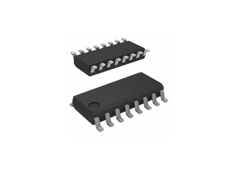
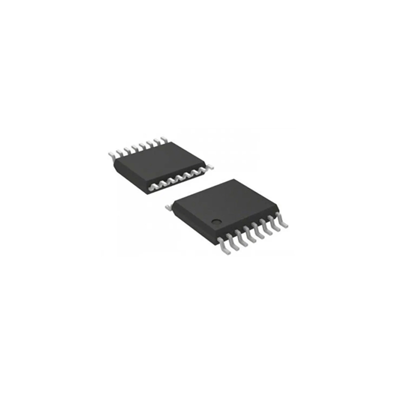
Order Information
| Ordering Name | Package | Manner of Packing | Minimum packing quantity |
| SSP1220 | TSSOP-16 | Reel | 4000 |