Features
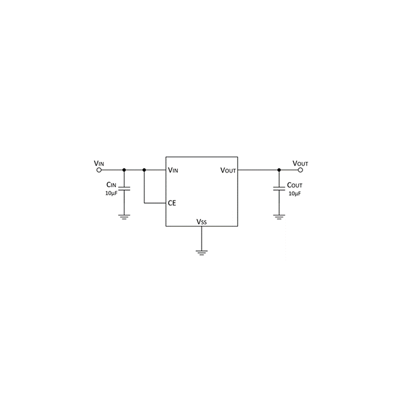
| Application
|
_画板-1@2x.png)


Absolute Maximum Ratings
(unless otherwise indicated, TA = 25 ° C.)
| Parameter | Symbol | Ratings | Units | |
| Input Voltage⑵ | Vin | -0.3~ 7 | V | |
| Output Voltage⑵ | Vout | -0.3~VIN+0.3 | V | |
| Output Current | Iout | 300 | mA | |
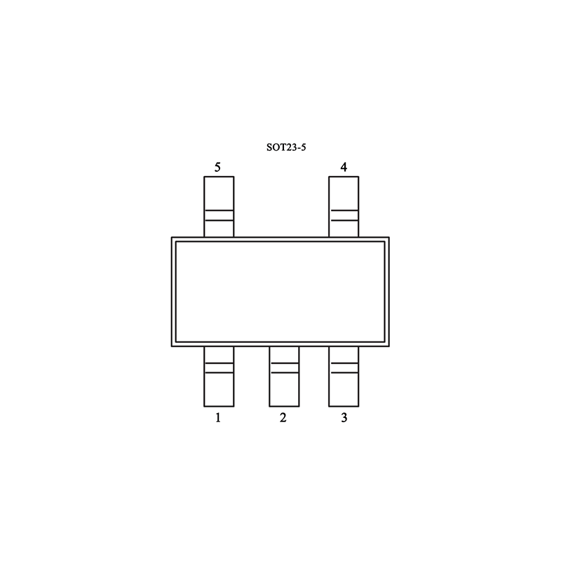
| Power Dissipation | SOT23-5 | PD | 400 | mW |
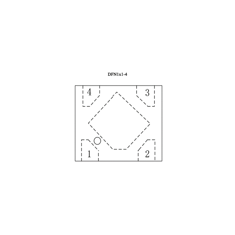
| DFN1x1-4 | 400 | mW | ||
| Operating Temperature Range⑶ | Ta | -40~85 | ℃ | |
| Junction Temperature Range⑷ | Tj | -40~125 | ℃ | |
| Storage Temperature Range | Tstg | -40~125 | ℃ | |
| Welding temperature and time | Tsolder | 260℃,10s | ||
| ESD | HBM | 4 | kV | |
| MM | 200 | V | ||
Note:
These are stress ratings only. Stresses exceeding the range specified under “Absolute Maximum Ratings” may cause substantial damage to the device. Functional operation of this device at other conditions beyond those listed in the specification is not implied and prolonged exposure to extreme conditions may affect device reliability.
All voltage values are obtained by reference.
H7211 can meet the performance specifications within the operating temperature range of 0℃ to 85℃. Beyond the operating temperature range of -40℃ to 85℃, the design and related parameters should be controlled to ensure.
H7211 in order to prevent damage to the product caused by overload current heating, built-in overtemperature protection circuit. When the node temperature rises to 125℃(typical value), the overtemperature protection circuit starts to work and stops the regulator. If the long-term work at the highest junction temperature will shorten the life of the product.
Electrical Characteristics
(unless otherwise indicated ,Vin=Vout+1V, Cin=Cout=1μF,Ta=25℃)
| Parameter | Symbol | Conditions | Min. | Typ. | Max. | Unit |
| Output Voltage | Vout (E) (7) | Iout=1mA | Vout (8) *0.98 | Vout (8) | Vout (8) *1.02 | V |
| Quiescent Current | Iss | Iout=0 | 30 | 60 | μA | |
| Shutdown Current | ISTBY | CE = VSS | 0.1 | μA | ||
| Output Current | Iout | - | 300 | mA | ||
| Voltage Drop | VDO(9) | Iout =150mA Vout≥2.8V | 150 | mV | ||
| Load Regulation | ΔVout | VIN= VoutT +1V, 1mA≤Iout≤100mA | 10 | mV | ||
| Line Regulation |  | Iout=10mA Vout +1V≤Vin≤6V | 0.01 | 0.2 | %/V | |
| Output voltage Temperature Characteristic |  | Iout =10mA -40≤T≤+85 | 100 | ppm/℃ | ||
| Short-circuit current | IShort | Vout =VSS | 100 | mA | ||
| Output Voltage | VIN | - | 2.0 | 6.0 | V | |
| PSRR F=217Hz | PSRR | IOUT = 50mA | 80 | dB | ||
| PSRR F=1kHz | 75 | dB | ||||
| PSRR F=10kHz | 70 | dB | ||||
| CE=HIGH | VCE“H” | 1.5 | VIN | V | ||
| CE=LOW | VCE“L” | 0.3 | V | |||
| Output Capacitor Discharge Resistor | RDISCHRG | VIN=5V, Vout=3.0V, VCE=VSS | 80 | Ω |
Description:
(6)Typical values are values at 25 ℃ and represent the most likely specifications.
(7)Vout (E): effective output voltage (when Iout keeps a certain value, VIN =(Vout +1.0V) output voltage).
(8)Vout: specified output voltage.
(9)VDO: Vin1 – Vout (E) ‘.
Vin1: The input voltage that gradually decreases when the output voltage drops to 98% of Vout (E)
Vout (E) ‘= Vout (E) * 98%
Order information
| Product model | Package | Manner of packing | Minimum packing quantity |
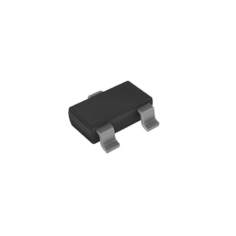
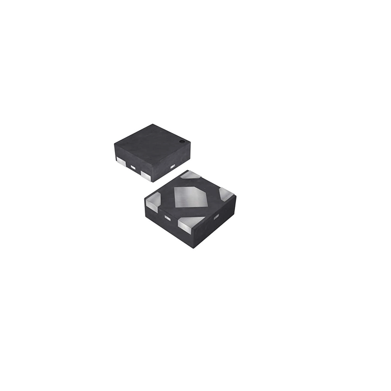
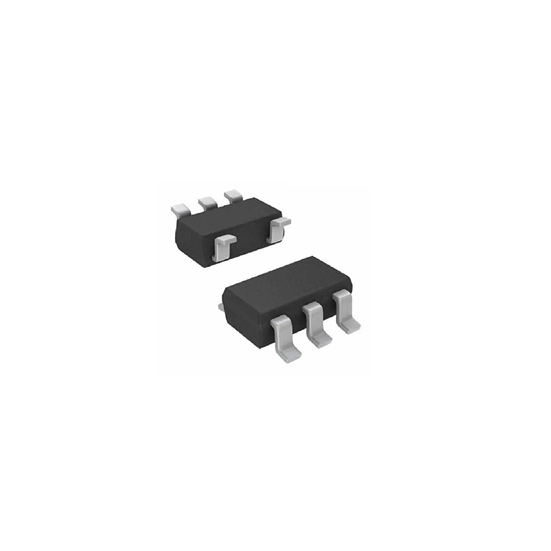
| H7211-XXM5R | SOT23-5 | Reel | 3000 |
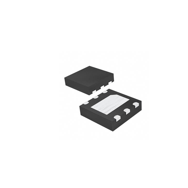
| H7211-XXDR | DFN1×1-4 | — | — |
Note: xx represents the output voltage value.
H7211-①②③④
| Designator | Symbol | Description |
| ①② | Integer | Output voltage Example:1.2V=①:1,②:2 |
| ③ | M5 | SOT23-5 |
| D | DFN1×1-4 | |
| ④ | R | RoHS / Pb Free |