_画板-1@2x.png)


Ⅰ、 Dreileiter-PT100-Temperaturmessprinzip
Der Hauptzweck der Drei-Draht-Verbindungsmethode besteht darin, den Einfluss des Leitungswiderstands auf die Messgenauigkeit zu eliminieren. Der Widerstandswert des PT100 ist sehr klein (100Ω @ 0℃), und der Widerstand der Anschlussdrähte (einige Zehntel Ohm bis einige Ohm, geschrieben als R6, R7, R15, siehe Dreidraht-RTD-Prüfschema) kann nicht zu vernachlässigende Fehler verursachen. Das Dreileitersystem löst dieses Problem durch ein cleveres Schaltungsdesign, bei dem alle drei Leitungen eines Dreileiter-RTDs in der Regel gleich lang sind. Unter der Annahme, dass der Widerstand der drei Leitungen gleich ist (RL1 = RL2 = RL3, d.h. R6=R7=R15 im Schaltplan), wird die interne Doppelstromquelle (IDAC) des SSP1220 verwendet, um die Auswirkungen dieser Leitungswiderstände auszugleichen.
Ausführliche Erläuterung des Messprinzips:
- Bei Verwendung zweier passender programmierbarer Stromquellen (IDAC1 und IDAC2) innerhalb des SSP1220, die denselben Strom ausgeben, wird empfohlen, die Stromquelle mit weniger als 1 mA auszuwählen; der Auswahlwert für diesen Test beträgt 500uA.
- Es wird angenommen, dass die drei Leitungswiderstände des PT100 gleich sind: R6 = R7 = R15 = Rl
- Der SSP1220 misst die Spannung am PT100 über ein differentielles Eingangspaar (AIN0, AIN1): VIN = VAIN1 - VAIN0
in Erwägung nachstehender Gründe VAIN1 = IIDAC1 x (RL1+RPT100) + (IIDAC1 + IIDAC2) x RL3, VAIN0 = IIDAC2 x RL2 + (IIDAC1 + IIDAC2) x RL3
Seit: IIDAC1 = IIDAC2 = IIDAC UND RL1 = RL2 = RL3 = RL
zu ersetzen: VIN = [IIDAC x (RL + RPT100) + 2IIDAC x RL] - [IIDAC x RL + 2IIDAC x RL] = IIDAC x RL + IIDAC x RPT100 + 2IIDAC x RL - 2IIDAC x RL = IIDAC x RPT100
Durch eine geschickte Schaltungskonfiguration wird der Einfluss des Leitungswiderstandes vollständig aus der differentiellen Eingangsspannung VIN eliminiert, und nur der Spannungsabfall über dem PT100-Widerstand wird berücksichtigt.
- Die SSP1220-Referenzspannung Vref wird durch die Zusammenführung von zwei IDAC-Strömen über einen hochpräzisen externen Referenzwiderstand, Rref (R5), erzeugt, d.h. Vref = (Iidac1 + Iidac2) * R
- Bei Verhältnismessungen ist der endgültige ADC-Ausgangscode proportional zu (Rpt100) / (Rref), unabhängig vom Absolutwert, der Genauigkeit und der Drift des IDAC-Stroms, wobei auch die Wirkung der Leitungswiderstände Rl1 und Rl2 ausgeglichen wird:
Für den 24-Bit SSP1220 lautet der numerische Ausgangscode:
Code = (223 - 1) x (VIN/VREF) = (223 - 1) x [RPT100/(2 x RREF) ]
Invertierung des PT100-Widerstandswertes durch ADC-Code:
RPT100 = [Code/(223-1)] x 2 x RREF
Schließlich wird Rpt100 entsprechend der Widerstands-Temperatur-Charakteristik von PT100 (in der Regel unter Verwendung der Callendar-Van Dusen-Gleichung oder der Tabellen-Nachschlagemethode) in einen Temperaturwert umgerechnet: T = f (Rpt100). Für den PT100 beträgt der Widerstandstemperaturkoeffizient bei 0℃, R0 = 100,00Ω ungefähr α≈ 0,00385 Ω/Ω/℃.
Ⅱ、Hardware-Schaltungsentwurf
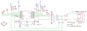
Gemäß der typischen Anwendung im Datenblatt sieht eine typische Dreileiter-PT100-Anschlussschaltung wie folgt aus:
- Anweisungen zum Anschluss des Stromkreises
- PT100-Anschluss: Der PT100 (Dreileitersystem) wird wie im Schaltplan dargestellt angeschlossen.
- Erzeugung einer Spannungsreferenz: Der IDAC1-Ausgang ist mit AIN2 verbunden (interne Softwarekonfiguration erforderlich), der IDAC2-Ausgang ist mit AIN3 verbunden (interne Softwarekonfiguration erforderlich), und die beiden IDAC-Ströme laufen am Knoten zusammen und fließen gemeinsam durch den externen Referenzwiderstand Rref(R5). Das andere Ende von REF ist mit der analogen Masse AVSS verbunden. Der positive Referenzeingang des SSP1220, REFP0, ist mit dem oberen Ende von RREF (R5) (dem IDAC-Zusammenführungspunkt) verbunden. Der negative Referenzeingang des SSP1220, REFN0, ist mit AVSS verbunden. Daher ist die Referenzspannung, VREF= (IIDAC1 + IIDAC2) * RREF.
- Signalmessung: AIN1 für SSP1220 ist als positiver Differenzeingang AINP konfiguriert und AIN0 des SSP1220 ist als negativer Differenzeingang AINN konfiguriert, so dass die gemessene Spannung die Potentialdifferenz zwischen AIN1 und AIN0 ist.
- Filterung der Schaltung: RC-Tiefpassfilter müssen sowohl an den Analogeingängen (AIN0, AIN1, AIN2) als auch an den Referenzeingängen (REFP0) zur Antialiasing- und Rauschunterdrückung hinzugefügt werden. Eingangsfilter: bestehend aus R1, R2, C1 und C6, C5. Referenzfilter: Besteht aus R3, R4, C2 und C3, C4. Um die Genauigkeit der Skalenmessungen zu erhalten, sollte die Grenzfrequenz des Referenzfilters mit der des Eingangsfilters übereinstimmen.
Ⅲ、Geräteauswahl und Parameterberechnung
Die hypothetischen Entwurfsziele sind wie folgt: PT100-Typ: Dreidraht; Temperaturmessbereich: -200°C ~ +850°C; Versorgungsspannung AVDD: 3,3V (AVSS = 0V); DAC-Strom: 500μA (pro Kanal); Datenrate: 20 SPS (für optimale Rauschleistung).
- Auswahl und Berechnung des Referenzwiderstands (Rref)
Rref ist das Herzstück der Genauigkeit des gesamten Systems. Funktion: Erzeugt die Referenzspannung V ref des ADC, deren Genauigkeit und Stabilität direkt die Messergebnisse bestimmen.
Widerstandsberechnung:
Um den Bereich des ADC zu maximieren und die Gleichtaktspannungsanforderungen des PGA zu erfüllen, wird die Vref normalerweise auf etwa die Hälfte der Versorgungsspannung eingestellt. In diesem Design ist AVDD = 3,3 V und die Ziel-VREF beträgt etwa 1,65 V.
IIDAC = I_IDAC1 + I_IDAC2 = 500uA + 500uA = 1mA
RREF = VREF /(IIDAC1 + IIDAC2) = 1,65V/1mA = 1,65kΩ
Es kann ein Widerstand mit einem Nennwert von 1,65 kΩ gewählt werden. Falls er nicht gefunden wird, sind auch 1,62 kΩ oder 1,69 kΩ ein akzeptabler Näherungswert.
Auswahlkriterien:
Genauigkeit: Mindestens ±0,1%, empfohlen ±0,05% oder höher für hochpräzise Anwendungen.
Temperaturschwankungen: Muss sehr gering sein, wobei ein Präzisionsfilmwiderstand von ±5 ppm/°C oder ±10 ppm/°C empfohlen wird.
Langfristige Stabilität: hoch.
Verwenden Sie niemals einen normalen 1%, 100ppm/°C Chip-Widerstand.
- IDAC-Strom und PGA-Verstärkungsoptionen
IDAC-Strom: 500μA ausgewählt. Dieser Wert stellt ein gutes Gleichgewicht zwischen Stromverbrauch, Selbsterhitzungseffekt und Signalamplitude dar. Wenn der Strom zu klein ist, ist das Signal schwach und wird leicht durch Rauschen beeinträchtigt; ein zu hoher Strom kann dazu führen, dass sich der PT100 selbst erwärmt oder die IDAC-konformen Spannungen überschreitet.
Auswahl der PGA-Verstärkung: Der PT100 hat eine kleinere Spannung (z. B. 500μA × 100Ω = 50mV), verwendet aber eine Verhältnismessung (die Referenzspannung stammt ebenfalls von IDAC), so dass keine Verstärkung erforderlich ist, um Sättigung zu vermeiden, und die Verstärkungsauswahl ist 1X.
- Auswahl der Komponenten des Filterkreises
Filterwiderstände (R1, R2, R3, R4): In der Regel wird 1kΩ gewählt. Dieser Wert ist groß genug, um effektiv zu filtern, und klein genug, um signifikante Offset-Spannungen am Eingang (aufgrund des Eingangsvorstroms) zu vermeiden. Sie dienen auch als Strombegrenzungsschutz.
Differenzialfilterkondensatoren (C1, C2): Stellen Sie die Grenzfrequenz zusammen mit dem Widerstand ein. Für eine Datenrate von 20SPS kann die Grenzfrequenz beispielsweise im Zehnerbereich von Hz eingestellt werden. fc = 1 / (2π * (R1+R2) * C1)。 Wenn R1+R2=2kΩ und fc ≈ 16Hz erwartet, ist C1 ≈ 1 / (2* 2000 * 16) ≈ 4,7μF. In realen Anwendungen werden häufig 100nF (0,1μF) verwendet, um eine größere Rauschunterdrückungsbandbreite zu erhalten. Typ: C0G (NPO) Keramikkondensatoren werden aufgrund ihrer stabilen Dielektrizitätskonstante, ihres niedrigen Spannungskoeffizienten und ihres geringen mikroakustischen Effekts empfohlen.
Gleichtaktgefilterte Kondensatoren (C5, C6, C3, C4): In der Regel eine Größenordnung kleiner als Differenzkondensatoren gewählt, z. B. 10nF, um sicherzustellen, dass Fehlanpassungen von Differenzkondensatoren nicht dazu führen, dass übermäßiges Gleichtaktrauschen in Differenzrauschen umgewandelt wird.
Ⅳ、Software-Konfiguration
- Master Logic:
float SSP1x20_read_temperature(void)
{
uint32_t ADC_data;
uint32_t ADC_temp1;
//SSP1x20_read_register(SSP1x20_REG0, 4, &Read_REGTab[0]);
Write_REGTab[0] = SSP1x20_MUX_AIN0_AIN1 | SSP1x20_GAIN_1 | SSP1x20_PGA_BYPASS_ON;
Write_REGTab[1]=SSP1x20_DR_20SPS|SSP1x20_MODE_NORMAL|SSP1x20_SC|SSP1x20_TS_ON| SSP1x20_BCS_OFF;
Write_REGTab[2]=SSP1x20_VREF_2048|SSP1x20_REJECT_OFF|SSP1x20_PSW_OFF | SSP1x20_IDAC_1000uA;
Write_REGTab[3] = SSP1x20_IDAC1_AIN2 | SSP1x20_IDAC2_AIN3 | SSP1x20_DRDYM_DRDY;
SSP1x20_WriteRegister(SSP1x20_REG0, 4, &Write_REGTab[0]);
SSP1x20_SendCommand(SSP1x20_CMD_START);
SPI_ADC_CS_LOW();
while (ADC_DRDY_GAIN == 1);//SSP1x20_DRDYM_DRDY
- Die Hauptkonfiguration und Beschreibung des Programms
- Konfigurieren von Register 0: MUX und Verstärkung
Write_REGTab[0] = SSP1x20_MUX_AIN0_AIN1 | SSP1x20_GAIN_1 | SSP1x20_PGA_BYPASS_ON;
| Bit | Konfiguration | Funktion | Beschreibung |
| BIT7~BIT4 | MUX_AIN0_AIN1 | Auswahl des Differenzeingangskanals | AIN0 - AIN1 → für PT100-Spannungsmessung |
| BIT3~BIT1 | GAIN_1(1x Verstärkung ) | Verstärkungseinstellungen | 1× (keine Verstärkung erforderlich, da Vin ≈ 1V) |
| BIT0 | PGA_BYPASS_ON | PGA-Umgehung | Schalten Sie den programmierbaren Verstärker aus, um Signalverzerrungen zu vermeiden. |
- Konfigurationsregister 1: Abtastrate und Modus
Write_REGTab[1] = SSP1x20_DR_20SPS | SSP1x20_MODE_NORMAL | SSP1x20_SC | SSP1x20_TS_OFF | SSP1x20_BCS_OFF;
| Bit | Konfiguration | Funktion | Beschreibung |
| BIT7~BIT5 | DR_20SPS | Datenrate | 20 mal/sec → geeignet für langsame Temperaturänderungen |
| BIT4~BIT3 | MODUS_NORMAL | Normaler Arbeitsmodus | Nicht einzeln oder fortlaufend |
| BITO | SC | Selbstkalibrierung aktiviert | Verbesserte Genauigkeit (empfohlen) |
| BIT1 | TS_OFF | Deaktivieren Sie den internen Temperatursensor | TS_ON schaltet den internen Temperatursensor ein, die Konfiguration zur Messung der externen Temperatur funktioniert nicht (diese Konfiguration hat die höchste Priorität) |
- Register 2 konfigurieren: Referenzspannung mit IDAC
Write_REGTab[2] = SSP1x20_VREF_2048 | SSP1x20_REJECT_OFF | SSP1x20_PSW_OFF | SSP1x20_IDAC_500uA;
| Bit | Konfiguration | Funktion | Beschreibung |
| BIT7~BIT6 | VREF_2048 | Externe Referenzspannung | Verwenden Sie einen externen R_REFR_REF, um eine Referenzspannung zu erzeugen (z. B. 1,65kΩ). |
| BIT5~BIT4 | REJECT_OFF | Keine Kerbfilterung | Es ist keine Störfestigkeit gegen Netzfrequenzstörungen erforderlich. |
| BIT3 | PSW_OFF | Aktivieren Sie den Netzschalter nicht | Aufrechterhaltung der normalen Stromversorgung |
| BIT2~BIT0 | IDAC_500uA | Erregerstrom | Auf 500 μA einstellen, um eine Überspannung von 3,9kΩ × 1mA = 3,9V > 3,3V zu vermeiden |
| Bit | Konfiguration | Funktion | Beschreibung |
| BIT7~BIT5 | IDAC1_AIN2 | IDAC1-Ausgang an AIN2 | Der Erregerstrom fließt durch das obere Ende des PT100 |
| BIT4~BIT2 | IDAC2_AIN3 | IDAC2-Ausgang an AIN3 | Rückkehr in den Pfad, um den Leitungswiderstand auszugleichen |
| BIT1 | DRDYM_DRDY | DRDY-Modus | Verwenden Sie das DRDY-Signal, um Ihnen mitzuteilen, dass die Konvertierung abgeschlossen ist. |
(4) Register 3 konfigurieren: IDAC-Routenkanal mit DRDY
- Dreidraht-PT100-Kern:
Aktueller Pfad:
- IDAC1 → AIN2 → PT100 → AIN1
- IDAC2 → AIN3 → AIN1(Rückgabe)
- Zwei Ströme sind gleich → Ausgleich des Spannungsabfalls am R_LEAD2R_LEAD2
uint32_t raw_u24 = SSP1x20_read_data_drdy();
SSP1220-Ausgänge 24-Bit-Datenaber MCUs lesen normalerweise in 32-Bit (SPI liest 4 Bytes auf einmal).
wenn (raw < 0) raw = -raw;
Die PT100-Spannung ist immer positiv (Strom fließt von AIN0 nach AIN1).
Wenn raw < 0 ist, wird die Die Softwarekonfigurationen von AIN0 und AIN1 sind vertauscht.
printf("Raw: %ld, R=%.3f Ω, Temp=%.2f °C\r\n", raw, R_pt100, temperature);
Drucken den ursprünglichen Codewert, berechnen den Widerstand und die Endtemperatur für einfache Fehlersuche
Wenn Raw negativ→ ist, wird die Konfiguration umgekehrt
Wenn R > 1400Ω → bedeutet dies, dass der IDAC oder Rref falsch eingestellt ist.
Wenn Temp = -999 → bedeutet dies, dass der R-Wert außerhalb des zulässigen Bereichs liegt.
Ⅴ、Messverfahren und Ergebnisse
- PT100-Spannungsmessprogramm an beiden Enden:
void SSP1x20_ADC_MeasurePt100(void)
{
float V_ref = 2.048; // Interne Referenzspannung 2.048V
//printf("\r\n Mehrpunkt-Einzelspannungsmessung \r\n");
Write_REGTab[0] = SSP1x20_MUX_AIN1_AIN0 | SSP1x20_GAIN_1 | SSP1x20_PGA_BYPASS_OFF;
Write_REGTab[1] = SSP1x20_DR_20SPS | SSP1x20_MODE_NORMAL | SSP1x20_SC | SSP1x20_TS_OFF | SSP1x20_BCS_OFF;
Write_REGTab[2] = SSP1x20_VREF_REF0 | SSP1x20_REJECT_OFF | SSP1x20_PSW_OFF | SSP1x20_IDAC_500uA;
Write_REGTab[3] = SSP1x20_IDAC1_AIN2 | SSP1x20_IDAC2_AIN3 | SSP1x20_DRDYM_DRDY;
SSP1x20_WriteRegister(SSP1x20_REG0, 4, &Write_REGTab[0]);
printf("Write_REGTab[0]=%x\r\n", Write_REGTab[0]);
printf("Write_REGTab[1]=%x\r\n", Write_REGTab[1]);
printf("Write_REGTab[2]=%x\r\n", Write_REGTab[2]);
printf("Write_REGTab[3]=%x\r\n", Write_REGTab[3]);
während (1)
{
SSP1x20_SendCommand(SSP1x20_CMD_START); // Wenn die kontinuierliche Messung aktiviert ist, wird dieser Befehl nur einmal gesendet
HAL_Delay(100);
SPI_ADC_CS_LOW();
}
SSP1220 Testergebnisse
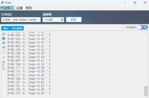
- SSP1220 interne Temperaturmessung
Interne Temperaturtestfunktion
float SSP1x20_read_temperature(void)
{
uint32_t ADC_data;
uint32_t ADC_temp1;
//SSP1x20_read_register(SSP1x20_REG0, 4, &Read_REGTab[0]);
Write_REGTab[0] = SSP1x20_MUX_AIN0_AIN1 | SSP1x20_GAIN_1 | SSP1x20_PGA_BYPASS_ON;
Write_REGTab[1] = SSP1x20_DR_20SPS | SSP1x20_MODE_NORMAL | SSP1x20_SC | SSP1x20_TS_ON | SSP1x20_BCS_OFF;
Write_REGTab[2] = SSP1x20_VREF_2048 | SSP1x20_REJECT_OFF | SSP1x20_PSW_OFF | SSP1x20_IDAC_1000uA;
Write_REGTab[3] = SSP1x20_IDAC1_AIN2 | SSP1x20_IDAC2_AIN3 | SSP1x20_DRDYM_DRDY;
SSP1x20_WriteRegister(SSP1x20_REG0, 4, &Write_REGTab[0]);
SSP1x20_SendCommand(SSP1x20_CMD_START);
SPI_ADC_CS_LOW();
while (ADC_DRDY_GAIN == 1);//SSP1x20_DRDYM_DRDY
Details zur Konfiguration des internen Temperaturtests:
Write_REGTab[1] = SSP1x20_DR_20SPS | SSP1x20_MODE_NORMAL | SSP1x20_SC | SSP1x20_TS_ON | SSP1x20_BCS_OFF;
- SSP1x20_TS_ON: Aktivieren Sie den internen Temperatursensor (kritisch), diese Konfiguration hat die höchste Priorität
- SSP1x20_SC: Selbstkalibrierung durchführen (empfohlen)
- 20SPS: Geringe Geschwindigkeit und hohe Genauigkeit, geeignet für Temperaturmessungen
Write_REGTab[2] = SSP1x20_VREF_2048 | SSP1x20_REJECT_OFF | SSP1x20_PSW_OFF | SSP1x20_IDAC_1000uA;
- SSP1x20_VREF_2048: Verwendung eine interne 2,048-V-Referenzspannung (nicht externer REF0!) )
- Da der interne Temperatursensor einen absoluten Spannungsausgang, a feste Referenzspannung muss zur Umrechnung der Temperatur verwendet werden.
- IDAC_1000uA: Obwohl IDAC aktiviert ist, IDAC im Modus TS_ON hat keinen Einfluss auf interne Temperaturmessungen (vernachlässigbar).
Write_REGTab[3] = SSP1x20_IDAC1_AIN2 | SSP1x20_IDAC2_AIN3 | SSP1x20_DRDYM_DRDY;
- Konfigurieren Sie den IDAC-Pin und DRDY, aber keinen Einfluss auf die interne Temperaturmessung haben (lassen Sie die Register einfach intakt).
- 2 Starten Sie die Konvertierung und warten Sie auf DRDY
SSP1x20_SendCommand(SSP1x20_CMD_START); SPI_ADC_CS_LOW();während (ADC_DRDY_GAIN == 1); // 等待 DRDY 变低
- Senden Sie den Befehl START, um einen kontinuierlichen Übergang zu starten.
- Warten auf den DRDY-Pin auf "low" zu setzenund zeigt damit an, dass die Daten bereit sind.
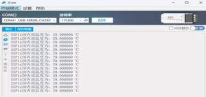
Die Messung der Innenraumtemperatur ist in der nachstehenden Abbildung dargestellt:
3. Externe Temperaturmessung (Methode 1, vereinfachte Berechnung des Faktors 0,385)
Code für externe Temperaturtests:
uint32_t ADC_gain_value = 0; // Auslesedaten
uint32_t ADC_value = 0; // Messung des Datenwerts
Float tmpPt100=0;
Schwimmer RTD=0;
void SSP1x20_ADC_Measure(void)
{
printf("\r\n Mehrpunkt-Einzelspannungsmessung \r\n");
Write_REGTab[0] = SSP1x20_MUX_AIN1_AIN0 | SSP1x20_GAIN_1 | SSP1x20_PGA_BYPASS_OFF; SSP1x20_MUX_AIN1_AIN0 Schnittstelle AIN1 AIN0 sollte anhand des aktuellen Schaltplans ausgewählt werden
Write_REGTab[1] = SSP1x20_DR_20SPS | SSP1x20_MODE_NORMAL | SSP1x20_SC | SSP1x20_TS_OFF | SSP1x20_BCS_OFF;
Write_REGTab[2] = SSP1x20_VREF_REF0 | SSP1x20_REJECT_OFF | SSP1x20_PSW_OFF | SSP1x20_IDAC_500uA;
Write_REGTab[3] = SSP1x20_IDAC1_AIN2 | SSP1x20_IDAC2_AIN3 | SSP1x20_DRDYM_DRDY;
SSP1x20_WriteRegister(SSP1x20_REG0, 4, &Write_REGTab[0]);
printf("Write_REGTab[0]=%x\r\n", Write_REGTab[0]);
printf("Write_REGTab[1]=%x\r\n", Write_REGTab[1]);
printf("Write_REGTab[2]=%x\r\n", Write_REGTab[2]);
printf("Write_REGTab[3]=%x\r\n", Write_REGTab[3]);
während (1)
{
SSP1x20_SendCommand(SSP1x20_CMD_START); Wenn die kontinuierliche Messung aktiviert ist, wird dieser Befehl nur einmal gesendet
HAL_Delay(100);
SPI_ADC_CS_LOW();
ADC_gain_value =0;
ADC_gain_value = SPI_ADC_ReadByte();
ADC_gain_value = (ADC_gain_value << 8) | SPI_ADC_ReadByte();
ADC_gain_value = (ADC_gain_value << 8) | SPI_ADC_ReadByte();
SPI_ADC_CS_HIGH();
RTD = 1650*( (float)ADC_gain_value /(0x3fffff));//Referenzwiderstand 1650 Ohm
tmpPt100 = (RTD-100)/0,38;
__NOP();
printf("R=%.3f Ω, Temp=%.2f °C\r\n",RTD, tmpPt100 );
}
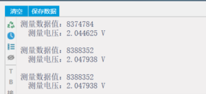
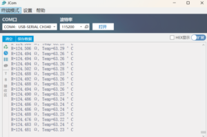
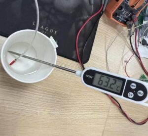
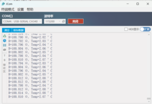
Die Ergebnisse der Drei-Linien-Widerstandsthermometer-Messung der Temperatur des Eis-Wasser-Gemischs sind in der nachstehenden Abbildung dargestellt:

Externe Temperaturmessungen (Methode zwei, berechnet nach der Callendar-Van Dusen-Gleichung) sind genauer
Master Code:
//Hochgenaues RTD -> Temperatur
static float rtd_to_temperature_iec60751(float rtd)
{
if (rtd < 0.0f) return -999.0f; // illegaler Wert
float t = (rtd - R0_PT100) / 0,385f; // Anfangsschätzung
if (rtd <= R0_PT100) {
//T < = 0°C: Verwenden Sie die vollständige Gleichung
for (int i = 0; i < 10; i++) {
float rt_calc = R0_PT100 * (1.0f + A_COEFF*t + B_COEFF*t*t + C_COEFF*(t - 100.0f)*t*t*t);
float dr_dt = R0_PT100 * (A_COEFF + 2.0f*B_COEFF*t + C_COEFF*(4.0f*t*t*t - 300.0f*t*t));
float error = rt_calc - rtd;
t -= Fehler / dr_dt;
if (fabsf(error) < 0.001f) break;
}
} sonst {
// T >= 0°C:: Verwenden Sie die vereinfachte Gleichung
for (int i = 0; i < 10; i++) {
float rt_calc = R0_PT100 * (1.0f + A_COEFF*t + B_COEFF*t*t);
float dr_dt = R0_PT100 * (A_COEFF + 2.0f*B_COEFF*t);
float error = rt_calc - rtd;
t -= Fehler / dr_dt;
if (fabsf(error) < 0.001f) break;
}
}
t zurückgeben;
}
/**
* @brief Analogkanal ADC-Messung (externe Temperaturmessung)
* @param Keine
* @retval Keine
*/
uint32_t ADC_gain_value = 0; // Auslesedaten
uint32_t ADC_value = 0; // Messung des Datenwerts
Float tmpPt100=0;
Schwimmer RTD=0;
void SSP1x20_ADC_Measure(void)
{
printf("\r\n Mehrpunkt-Einzelspannungsmessung \r\n");
Write_REGTab[0] = SSP1x20_MUX_AIN1_AIN0 | SSP1x20_GAIN_1 | SSP1x20_PGA_BYPASS_OFF;
Write_REGTab[1] = SSP1x20_DR_20SPS | SSP1x20_MODE_NORMAL | SSP1x20_SC | SSP1x20_TS_OFF | SSP1x20_BCS_OFF;
Write_REGTab[2] = SSP1x20_VREF_REF0 | SSP1x20_REJECT_OFF | SSP1x20_PSW_OFF | SSP1x20_IDAC_500uA;
Write_REGTab[3] = SSP1x20_IDAC1_AIN2 | SSP1x20_IDAC2_AIN3 | SSP1x20_DRDYM_DRDY;
// Write_REGTab[3] = SSP1x20_IDAC1_AIN3 | SSP1x20_IDAC2_AIN2 | SSP1x20_DRDYM_DRDY;
SSP1x20_WriteRegister(SSP1x20_REG0, 4, &Write_REGTab[0]);
printf("Write_REGTab[0]=%x\r\n", Write_REGTab[0]);
printf("Write_REGTab[1]=%x\r\n", Write_REGTab[1]);
printf("Write_REGTab[2]=%x\r\n", Write_REGTab[2]);
printf("Write_REGTab[3]=%x\r\n", Write_REGTab[3]);
während (1)
{
SSP1x20_SendCommand(SSP1x20_CMD_START); Wenn die kontinuierliche Messung aktiviert ist, wird dieser Befehl nur einmal gesendet
HAL_Delay(100);
SPI_ADC_CS_LOW();
ADC_gain_value =0;
ADC_gain_value = SPI_ADC_ReadByte();
ADC_gain_value = (ADC_gain_value << 8) | SPI_ADC_ReadByte();
ADC_gain_value = (ADC_gain_value << 8) | SPI_ADC_ReadByte();
SPI_ADC_CS_HIGH();
#define CALIBRATED_FULL_SCALE 4210300.0f // entsprechend den Kalibrierungsdaten
RTD = 1650.0f * ((float)ADC_gain_value / CALIBRATED_FULL_SCALE);
tmpPt100 = rtd_to_temperature_iec60751(RTD);
__NOP();
printf("R=%.3f Ω, Temp=%.2f °C\r\n",RTD, tmpPt100 );
}
}
Die Testergebnisse sind in der Abbildung dargestellt:
Prüfung der Warmwassertemperatur:
Test der Eis-Wasser-Mischung:

4. Details zur Konfiguration des externen Temperaturtests:
| Register | Werte konfigurieren (Ihr Code) | Beschreibung der Funktion: | Warum haben Sie dies gewählt? |
| REG0 Write_REGTab[0] | SSP1x20_MUX_AIN1_AIN0 | SSP1x20_GAIN_1 |SSP1x20_PGA_BYPASS_OFF | Kanalauswahl + Verstärkungseinstellungen eingeben | |
| SSP1x20_MUX_AIN1_AIN0 | Differenzeingänge: AIN1 ist positiv und AIN0 ist negativ | Der PT100 wird beidseitig an AIN0 und AIN1 angeschlossen und benötigt eine Differenzspannungsmessung. ⚠️ Beachten Sie die PolaritätWenn die Konfiguration umgekehrt ist, gibt der ADC einen negativen Wert aus (z. B. 0x800000), was zu einer negativen Temperatur führt. | |
| SSP1x20_GAIN_1 | Verstärkung = 1 | Der PT100 hat eine kleinere Spannung (z. B. 500μA × 100Ω = 50mV), verwendet aber eine Verhältnismessung (die Referenzspannung stammt ebenfalls von IDAC), so dass keine Verstärkung ist erforderlich, um eine Sättigung zu vermeiden. | |
| SSP1x20_PGA_BYPASS_OFF | Kein Bypass PGA | Behalten Sie die PGA-Funktion bei (auch wenn die Verstärkung 1 ist), um sicherzustellen, dass der Signalweg normal ist. | |
| REG1 Write_REGTab[1] | SSP1x20_DR_20SPS | SSP1x20_MODE_NORMAL | SSP1x20_SC | SSP1x20_TS_OFF | SSP1x20_BCS_OFF | Datenrate + Betriebsart | |
| SSP1x20_DR_20SPS | Abtastrate = 20 Abtastpunkte/Sekunde | Eine niedrige Geschwindigkeit verbessert die Genauigkeit, unterdrückt Rauschen und eignet sich für Temperaturmessungen (langsame Änderungen). | |
| SSP1x20_MODE_NORMAL | Normaler kontinuierlicher Umwandlungsmodus | Kontinuierliche Datenausgabe für die Echtzeitüberwachung. | |
| SSP1x20_SC | Selbstkalibrierung durchführen | Die Kalibrierung nach jeder Konfiguration beseitigt Offset-/Verstärkungsfehler und verbessert die Genauigkeit. | |
| SSP1x20_TS_OFF | Schalten Sie den internen Temperatursensor aus. | Wir messen den externen PT100 und benötigen die interne Temperatur nicht. | |
| SSP1x20_BCS_OFF | Abbrandstromquellen deaktivieren | Nein, das müssen Sie nicht. | |
| REG2 Write_REGTab[2] | SSP1x20_VREF_REF0 | SSP1x20_REJECT_OFF | SSP1x20_PSW_OFF SSP1x20_IDAC_500uA | Referenzspannung + IDAC-Einstellungen | |
| SSP1x20_VREF_REF0 | Verwenden Sie eine externe Referenz Spannung (REF0 = Spannung zwischen AIN2/AIN3). | Umsetzung verhältnisbasierte Messungen: ADC-Ergebnis = (Vpt100 / Vref) × 224, unabhängig vom IDAC-Strom absolutnur auf Rref bezogen, resistent gegen Schwankungen der Stromversorgung. | |
| SSP1x20_REJECT_OFF | 50/60Hz-Unterdrückung ist nicht aktiviert | Wenn die Umgebungsstörung gering ist, kann sie ausgeschaltet werden; wenn sie sich in einer Netzfrequenzumgebung befindet, wird empfohlen, REJECT_50 einzuschalten. | |
| SSP1x20_PSW_OFF | Schalten Sie den Schalter für die Stromversorgung des Sensors aus. | Der PT100 wird über IDAC versorgt und benötigt kein zusätzliches PSW. | |
| SSP1x20_IDAC_500uA | Konstantstromquelle Strom einstellen = 500 μA | Gemeinsame Stromwerte, Ausgleich der Leistungsaufnahme und der Signalamplitude (100Ω → 50mV). | |
| REG3 Write_REGTab[3] | SSP1x20_IDAC1_AIN2 | SSP1x20_IDAC2_AIN3 | SSP1x20_DRDYM_DRDY | IDAC-Ausgangspin + DRDY-Konfiguration | |
| SSP1x20_IDAC1_AIN2 | IDAC1-Ausgang an AIN2 | AIN2 bis PT100 (Erregung) | |
| SSP1x20_IDAC2_AIN3 | IDAC2-Ausgang an AIN3 | AIN3 ist mit dem Referenzwiderstand an einem Ende von R_ref verbunden (bildet die Schleife) → verwirklicht Dreidrahtkompensation (kompensiert den Leitungswiderstand). | |
| SSP1x20_DRDYM_DRDY | Aktivieren Sie den DRDY-Stift (Datenbereitschaftssignal). | Die MCU erkennt DRDY-Low-Pegel über GPIO, um zu wissen, wann Daten gelesen werden und um Polling zu vermeiden. |
----------------------------------
Schlüsselteil Code Formelberechnung:
RTD = 1650*( (float)ADC_gain_value /(0x3fffff)); //Referenzwiderstand 1650 Ohm tmpPt100 = (RTD-100)/0,385;
Bezugswiderstand 1650 Ohm,
Erste Zeile Code RTD = 1650 * (ADC / 0x3FFFFF)
Entwickelt, um den ursprünglichen ADC-Wert in den Widerstandswert des PT100 umzuwandeln (Verhältnismessung)
- VIN = I × RPT100 (Spannung über PT100)
- VREF = I × RREF (Spannung am Referenzwiderstand)
An beiden Enden wird die gleiche Konstantstromquelle I adc verwendet
Also: Vin/Vref = Rpt100/Rref
Der Ausgang des ADC ist das digitalisierte Ergebnis dieses Verhältnisses
ADC_Code = Vin/Vref x 224
So zurückgedrängt
Rpt100= Rref x ADC_Code /224
---------------------------------------
Zweite Codezeile: tmpPt100 = (RTD - 100) / 0,385;
Schätzen Sie die Temperatur mit einer linearen Näherungsformel
Bei 0°C, Rpt100 = 100 Ω
Bei jeder Temperaturerhöhung um 1°C steigt der Widerstand um etwa 0,385 Ω.
Also
T ≈ (R-100)/0.385
Ⅵ、 Anleitung zur Fehlersuche bei allgemeinen Problemen
| Anomal | Mögliche Ursachen | Schritte zur Fehlersuche |
| Der ursprüngliche Wert des ADC (raw) ist negativ | AIN0 ist das Gegenstück zur AIN1-Konfiguration | 1. Überprüfen Sie, ob die Softwarekonfiguration mit der Verbindung zur Hardware übereinstimmt |
| R_PT100 > 1400Ω | 1. Falsche IDAC-Stromkonfiguration; 2. Rref öffnet | 1. Prüfen Sie die IDAC-Konfiguration von REG2 (stellen Sie sicher, dass sie 500μA beträgt); 2. messen Sie den Widerstandswert R ref mit einem Multimeter, um zu bestätigen, dass der Stromkreis nicht offen ist |
| Der Temperaturwert ist - 999°C | PT100 überschreitet den Bereich 18Ω~330Ω | 1. Prüfen Sie, ob der PT100 nicht angeschlossen ist (messen Sie den PT100-Widerstand); 2. überprüfen Sie die SPI-Kommunikation (Lesen der Registerkonfigurationswerte) |
| Temperaturschwankungen > 0,1°C | 1. Große Restwelligkeit der Stromversorgung; 2. elektromagnetische Störungen | 1. SSP1220 VDD-Welligkeit messen (≤ 10mV erforderlich); 2. Prüfen Sie die Erdung des Abschirmdrahtes, um Störungen zu vermeiden. |
Ⅶ、 SSP1220 Core Register Konfigurationstabelle
| Register | Artikel konfigurieren | Wert (externe Temperaturmessung) | Beschreibung der Funktion: |
| REG0 | Differenzielle Kanäle | AIN1-AIN0 | Passen Sie die PT100-Verdrahtung an, um negative Rohdaten zu vermeiden. |
| gewinnen | 1× | Vermeidung von Signalsättigung und Anpassung an die Verhältnismessung | |
| PGA-Umgehung | deaktivieren | Bewahrung der Integrität des Signalwegs | |
| REG1 | Abtastrate | 20SPS | Niedrige Geschwindigkeit verbessert die Genauigkeit und passt sich an langsame Temperatursignale an |
| Arbeitsmodus | Normaler Modus | Kontinuierliche Umwandlung und Echtzeitausgabe von Temperaturdaten | |
| Selbstkalibrierung | aktivieren. | Beseitigung von Offset-/Gain-Fehlern und Verbesserung der Genauigkeit | |
| Interner TS | deaktivieren | Externe Temperaturmessung erfordert keine internen Sensoren | |
| REG2 | Referenzspannung | Externer REF0 | Ratio-basierte Messung zum Ausgleich von IDAC-Stromschwankungen |
| IDAC-Strom | 500μA | Symmetrische Leistungsaufnahme und Signalamplitude (50mV 100Ω) | |
| REG3 | IDAC1-Routen | AIN2 | Der Erregerstromeingang PT100 |
| IDAC2-Routen | AIN3 | Dem Vorwiderstand R7 entgegenwirken |
Tabelle der Koeffizienten der Ⅷ、Callendar-Van Dusen-Gleichung
| Koeffizient | Numerischer Wert | Einheit | Umfang der Anwendung |
| R0 | 100.0 | Ω | 0°C Bezugswiderstand |
| A | 3.9083×10⁻³ | ℃-1 | -200℃~600℃ |
| B | -5.775×10⁻⁷ | ℃-2 | -200℃~600℃ |
| C | -4.183×10⁻¹² | ℃-4 | -200℃~0℃ |
Den vollständigen Code erhalten Sie, wenn Sie sich an unseren technischen Support wenden. Kontakt: 18014203727

