Features
| Applications
|
Blog
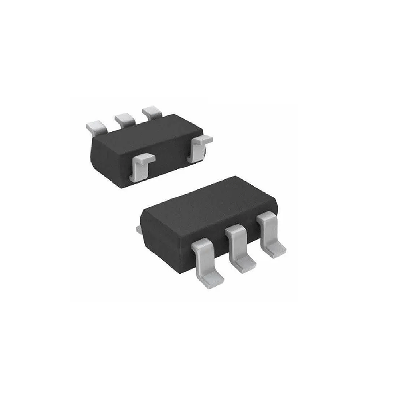
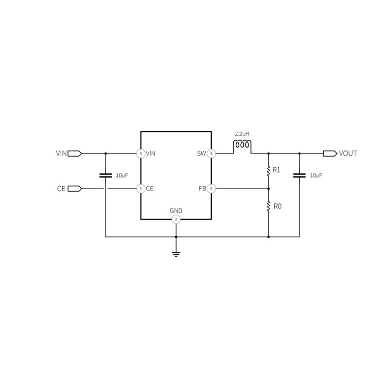
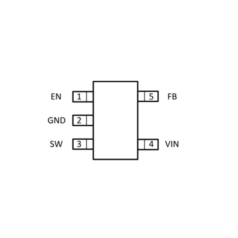


Features
| Applications
|
| Item | Min | Max | Unit |
| VIN voltage(1) | -0.3 | 6.0 | V |
| VOUT voltage (1) | -0.3 | 5.5 | V |
| Continuous Power Dissipation (TA = 25°C) (2) | 0.4 | W | |
| Power dissipation | Internally Limited | ||
| Operating junction temperature, TJ | -40 | 125 | °C |
| Storage temperature, Tstg | –65 | 150 | °C |
| Lead Temperature (Soldering, 10sec.) | 260 | °C | |
| Symbol | Parameter | Max. | Unit |
| θJA | Thermal Resistance(3) | 170 | ℃/W |
| θJC | 75 | ℃/W |
Note (1): Exceeding these ratings may damage the device.
Note (2): The maximum allowable power dissipation is a function of the maximum junction temperature TJ(MAX), the junction-toambient thermal resistance θJA, and the ambient temperature TA. The maximum allowable continuous power dissipation at any ambient temperature is calculated by PD(MAX)=(TJ(MAX)-TA)/θJA. Exceeding the maximum allowable power dissipation will cause excessive die temperature, and the regulator will go into thermal shutdown. Internal thermal shutdown circuitry protects the device from permanent damage.
Note (3): Measured on JESD51-7, 4-layer PCB.
VIN=5V,TA=25°C,unless specified otherwise.
| Parameter | Test Conditions | Min | Typ | Max | Unit |
| Input Voltage Range | 2.7 | 5.5 | V | ||
| Input over voltage protection | 5.8 | 6 | 6.5 | V | |
| Quiescent current, IQ | VIN =5.0V | 20 | 40 | 60 | µA |
| Shutdown current, IOFF | VIN =5.0V , VCE =0 | 0.1 | 2.0 | µA | |
| Input voltage UVLO | Rising | 2.55 | 2.65 | V | |
| Falling | 2.25 | 2.37 | V | ||
| Feedback Voltage | VIN =5.0V | 0.588 | 0.6 | 0.612 | V |
| Output current Limit | VIN = 5.0V, VOUT = 3.3V | 2.5 | 3 | A | |
| Line regulation | VIN = 3 to 5.0V | 0.2 | %/V | ||
| Load regulation | IOUT= 0.1 – 1A | 0.1 | 2 | %/A | |
| Switching frequency | VIN =5.0V | 1 | 1.3 | 1.8 | MHz |
| ON resistance PMOS | VIN =5.0V | 140 | mΩ | ||
| ON resistance NMOS | VIN =5.0V | 80 | mΩ | ||
| CE input threshold ON | VIN =5.0V | 0.9 | 1.1 | V | |
| CE input threshold OFF | VIN =5.0V | 0.4 | 0.7 | V | |
| CE input pull down resistor | 750 | kΩ | |||
| Output discharge resistor, Rpd | VIN =5.0V | 50 | Ω | ||
| Over temperature protection | 150 | ℃ | |||
| OTP hysteresis | 40 | ℃ |


Shanghai Siproin
Microelectronics Co.,Ltd.
Welcome your contact.