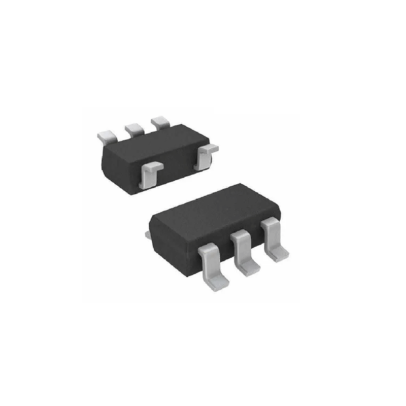
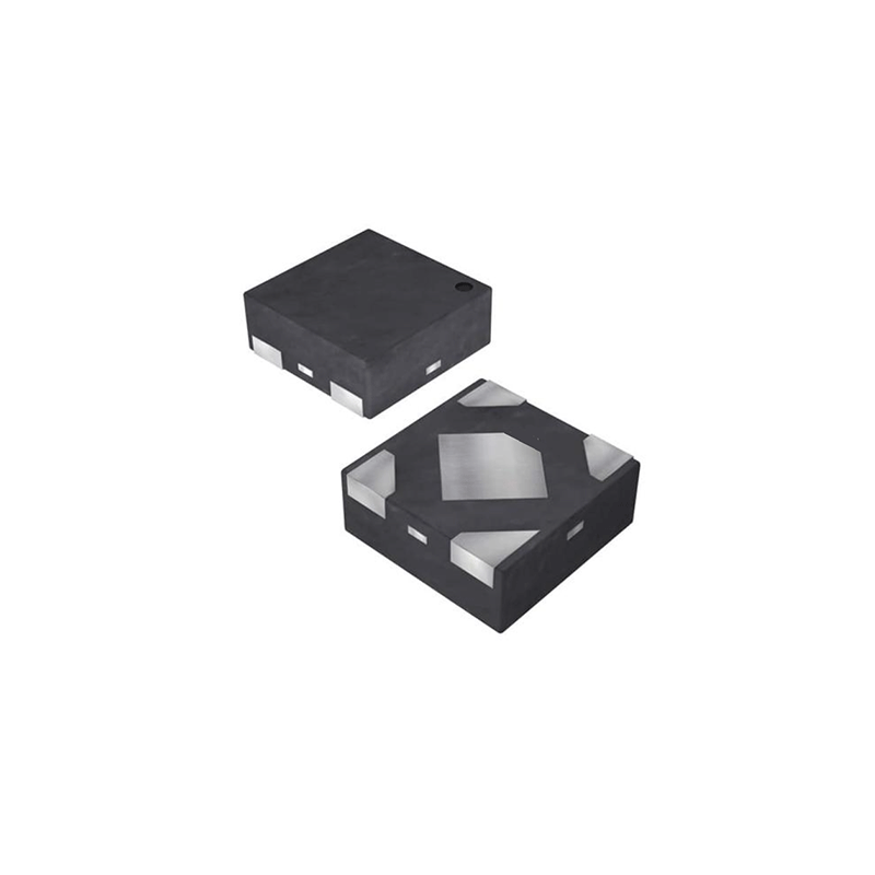
During electronic design, we always need different DC voltages to provide circuit work. The most commonly used one is to use LDO voltage regulator chips to achieve the output of different DC voltages. So how to choose a suitable LDO is particularly important. Many engineers during selecting progress, they only select based on the two indicators of output voltage and current, but ignoring several other key technical indicators, resulting in the selected LDO is not the best choice. Let’s learn about the working principle of LDO and several important technical indicators.
Principle Introduction
LDO,as know as Low Dropout Regulator,Belongs to linear power supply. The application requires relatively few external components. Most models of LDO only need to connect a filter capacitor at the input end and the output end. As shown below:

Its internal structure is shown in the figure below:

From the schematic diagram we can know LDO is mainly composed of PMOS, error amplifier, feedback resistor and base reference voltage.LDO main working process is to divide the output voltage through a voltage dividing resistor, compare it with the base reference voltage, and adjust the conduction voltage drop of the PMOS tube through the op amp output to perform dynamic output voltage stabilization.
Selection parameters
- Input Voltage
Input voltage refers to the operating voltage range that can be input at the input terminal. If the input voltage is 5V, then when selecting, we should choose an LDO with a withstand voltage of about 10V. Generally, the input voltage range is recommended to be more than twice the normal input voltage.
- Vout
Output voltage is the most important parameter of an LDO, and it is also the first parameter that electronic equipment designers should consider when selecting a voltage regulator. LDOs are available in fixed output voltage and adjustable output voltage types. Fixed output voltage regulators are easier to use, and because the output voltage is precisely adjusted by the manufacturer, the regulator has high accuracy. However, the output voltage values set by it are common voltage values, which cannot meet all application requirements. The output accuracy of the adjustable output LDO is affected by the accuracy of external components and temperature changes.
- Max Current
It is the maximum output current value of the output terminal. The average and peak currents during normal operation should be taken into consideration here. It mainly depends on whether the LDO can provide the required peak current in a short time.
- Pd
LDO Simple formula for dissipated power PD=(Vin-Vout)*Iout,Assume input voltage Vin=12V,The output voltage Vout=3.6V,Output current Iout=180mA ,then LDO Dissipated power PD=1.512W,All this power consumption is through heat loss, so it is not recommended for LDO to be used in scenarios where the input and output voltage difference is too large and the output current is large.
If we really need to use it, we have to consider how much power consumption the LDO chip can withstand. For details, please refer to the data provided in the chip manual.
Let’s take SSP7903 as an example. The figure below shows the maximum power dissipation of different packages. This maximum power dissipation is the maximum thermal power consumption that the chip can withstand. If it exceeds it, it will burn out. At the same time, we recommend not to use it for a long time at the maximum limit value.
| Dissipated power PD | SOT89 1000 SOT223 1500 TO252 1800 | mW |
The typical package above dissipates power, so we will choose the bottom TO 252 package. There should be a margin when designing. You can increase the heat dissipation pad or add a heat sink to reach the temperature and increase power, so as not to burn out the LDO chip.
- Dropout Voltage
Vdrop=Vin-Vout,Defined as the difference between the input voltage and the output voltage。LDO has different voltage differences under different load currents. The figure below is the relationship curve between output current and voltage difference. It can be seen that the smaller the output current, the smaller the voltage difference. The lower the input voltage, the lower the power dissipation, improving efficiency. If during actual application, the voltage difference between the input voltage and the output voltage is very small, but a certain current (100mA) needs to be output, then a suitable LDO must be selected to ensure normal output.
For example, the voltage difference of a 78L05 is about 2V, while the voltage difference of the H7550-H is only about 600mV. Of course, only by choosing H7550-H can the output be guaranteed to be normal. At the same time, the power dissipation of the chip will be much smaller, and the performance will be better.

- Iq
Iq=Iin-Iout,It is defined as the current required to power the LDO internal circuit when the external load current is 0. The Iq of most MOS structure LDOs is very small, which is an important indicator to measure the LDO’s own consumption under low load conditions. The smaller the Iq, the better.
- Load Transient Response
Represents the maximum change in output voltage caused by sudden changes in load current. It is a function of the output capacitance, its equivalent series resistance and bypass capacitance. The function of the output capacitor is to improve the load transient response capability and also serves as a high-frequency bypass.

- Power Up
It refers to the phenomenon that when a certain load is applied at the moment of power-on, the voltage at the output terminal exceeds the accuracy range. This is also a point that many people ignore. If the overshoot value is large, it may affect or even damage the subsequent circuit components, causing circuit board failure.
This is an LDO chip bought on a certain website. The input voltage is 7V, the load is 10mA, and the output voltage is 5V. The power-on waveform and voltage switching waveform are as follows:


Power-on instant waveform Voltage switching waveform (7V to 10V switching)
The maximum value at the moment when the chip is powered on reaches 6.816V, lasting 263ms, exceeding more than 36%. When the voltage is switched, the maximum value reaches 6.225V, lasting 1ms, exceeding more than 24%. For those 5V microcontrollers It is a big damage, which will cause damage to the subsequent chip with a high probability.
The SSP7903 has used before has an input voltage of 5.6V, a load of 10mA, and an output of 3.6V. There is no overshoot during power-on and voltage switching.。


Power-on instant waveform Voltage switching waveform (5.6V to 15V switching)
- Power supply rejection ratio(PSRR)
The power supply ripple rejection ratio is the ratio of the input voltage noise fluctuation (ripple) to the output voltage noise fluctuation (ripple), commonly expressed in decibels (dB),
The formula is ![]() ,Defined as the LDO’s ability to suppress noise on Vin.
,Defined as the LDO’s ability to suppress noise on Vin.
The larger the value of PSRR, the better the ripple suppression capability.
- Noise
Different from PSRR, noise refers to the noise signal generated by the LDO itself. A low-noise LDO voltage regulator chip can effectively reduce the additional noise generated by the LDO. The output voltage is purer. The calculated value of noise is generally the effective value (rms). , you can also use peak to peak to analyze.
- Output Efficiency
![]() ,Since Iq is very small, it can be ignored in actual calculations.
,Since Iq is very small, it can be ignored in actual calculations.
It can be seen from the formula that the greater the voltage difference between Vin and Vout, the lower the efficiency of the LDO, the greater the power it consumes and the greater the heat it generates.
- Load Regulation
It refers to the change in output voltage under a given load change, where the load change is usually from no load to full load. The smaller the load regulation rate, the better.

- Line Regulation
It refers to the impact of input changes on the output, that is, the ratio of the output voltage change to the input voltage change under a certain load. The smaller the linear adjustment rate, the better.
LDO voltage regulator chip typical application circuit reference
- circuit to increase output voltage

- constant current regulation circuit

- Dual power output circuit

The following are frequently used LDO :
| Modle No | Input voltage(V) | Output voltage(V) | Quiescent Current μA | Maximum output current(mA) |
| SSP9193 | 5.5 | 1.2V~5.0 | 20 | 400 |
| SSP7935 | 35 | 2.5V~5.0 | 1.6 | 200 |
| SSP7903 | 40 | 3V~12.0 | 1.6 | 1000 |
| H75XX-H | 45 | 2.5V~5.0 | 2.5 | 100 |
| SSP7985 | 80 | 2.5V~5.0 | 2 | 150 |
Company Profile:Siproin Microelectronics Co., Ltd. is a professional “fabless” company engaged in integrated circuit development and providing system-level solutions. The company’s main products include magnetic storage STT-MRAM, power management, IoT communications, dedicated drivers, industrial metering, and single chip microcomputer (MCU). /DSP) and corresponding solutions, official website: http://www.siproin.com
_画板-1@2x.png)


