_画板-1@2x.png)

Introduction:
In modern industrial measurement and automation control, resistive bridge sensors are widely used in the detection of physical quantities such as weight, pressure, and strain due to their high accuracy and stability. However, how to design a high-performance resistance bridge measurement system and ensure its reliability and accuracy in practical applications is a challenge faced by many engineers and technicians.
This article takes the SSP1X20-resistance bridge measurement application as an example, and introduces in detail the complete technical solution from hardware circuit design, device selection, parameter calculation to software implementation. Through the fundamentals of Wheatstone bridges, how strain gauge load cells work, and the application of proportional measurement techniques, we delve into how to optimize system performance and provide solutions to common problems.
Whether you are an electronics engineer, embedded developer, or enthusiast interested in high-precision measurement technology, this article will provide you with practical technical references and implementation ideas. Next, we will start with an overview of the principles and analyze the design and implementation of this system step by step.
1. Principle Overview:
1.1 The basic working principle of the Wheatstone bridge
The Wheatstone bridge consists of four resistors in a balanced circuit, and its basic structure is as follows:

Equilibrium condition: When R1/R2 = R3/R4, the bridge is balanced, Vout = 0
Output Voltage:
Working principle:
Voltage distribution: The supply voltage Vs of the bridge is applied at both ends of the bridge, and the current is distributed through resistors R1, R2, R3, and Rx (resistance to test). The equilibrium state of the bridge means that the voltages of the two branches are equal and the output voltage is zero.
Measurement Principle: The core idea of the Wheatstone bridge is to reflect changes in resistance by measuring changes in voltage. When the resistance changes, the bridge is no longer balanced and the galvanometer shows the current, so that the change in resistance can be deduced by the change in current.
1.2 Strain gauge load cell principle
The working principle of resistance strain gauges is based on the strain effect, that is, when the conductor or semiconductor material produces mechanical deformation under the action of external force, its resistance value changes accordingly, which is called “strain effect”. Semiconductor strain gauges are made of semiconductor materials, and their working principle is based on the piezoresistive effect of semiconductor materials. The piezoresistive effect refers to the phenomenon that the resistivity of a semiconductor material changes when it is subjected to an external force in a certain axis. The strain gauge is a component composed of sensitive gratings for measuring strain, which is firmly pasted on the measuring point of the component when used, and the strain of the measuring point after the component is stressed, and the sensitive grating is also deformed and its resistance changes, and then the change of resistance is measured by a special instrument, and converted into the strain value of the measuring point. There are many varieties and forms of metal resistance strain gauges, including wired resistance strain gauges and foil resistance strain gauges. Foil resistive strain gauge is a sensitive element made based on the strain-resistance effect, using metal foil as a sensitive gate, which can convert the strain variable of the test piece into a change in resistance.
1.3 Principle of proportional measurement
Key benefits: Use the same excitation source as sensor power supply and ADC reference.
Transfer function: Digital output code ∝ (Vsensor / Vexcitation) × gain
Error offset mechanism: excitation voltage drift affects both sensor output and reference voltage; cancel each other out in ratio calculations; Common mode errors such as temperature drift and power supply noise are eliminated.
2. Hardware circuit design
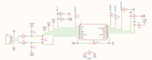
- Anweisungen zum Anschluss des Stromkreises
- The digital input and output pins (CS, SCLK, DIN, DOUT/DRDY, DRDY do not need to be used) are connected in series with a 47Ω resistor that allows for smooth transition, suppression of overshoot, and some form of overvoltage protection.
- Using an external reference, channel 0 is selected, and the reference voltage is 5V.
- AIN0/REFP1 and AIN1 are suspended to minimize leakage current from the analog input.
- Connect the CLK to GND to avoid excessive leakage current from the power supply.
- SIPROIN recommends that the differential capacitor (C2) should be at least an order of magnitude (10x) higher than the common-mode capacitor (C1, C3) because the mismatch of the common-mode capacitance can cause the common-mode noise to be converted to differential noise, which is configured as follows: R17 = R18 = 1kΩ, C2 = 100nF, C1 = C3 = 10nF.
- Capacitors C8 and C7 use multilayer ceramic chip capacitors (MLCCs) to provide equivalent series resistance (ESR) and inductance (ESL) characteristics to achieve power decoupling.
3. Device selection and parameter calculation
3.1 Core Device Selection Table
| Devices | Specifications | quantity | Selection basis |
| ADC chip | SSP1220, TSSOP-16 | 1 | 24-bit Δ-SIGMA ADC with integrated PGA |
| Input filter resistor | R17=R18=1KΩ,0805 | 2 | Current limiting protection, filtering |
| Enter the differential capacitor | C2=100nF, X7R,50V,0805 | 1 | Differential noise filtering |
| Input common mode capacitors | C1=C3=10nF, X7R,50V,0805 | 2 | Common-mode noise suppression |
| decoupling capacitors | C7=C8=100nF, X7R,16V,0603 | 2 | Low ESR/ESL MLCC |
| External reference source | 5V±0.1% | 1 | High-precision benchmarks |
3.2 Parameter calculation
3.2.1 Digital Interface Resistance Calculation
(1) Analysis of 47Ω resistance:
Main functions: suppress signal overshoot and ringing; Provides limited overvoltage protection; Slow signal edges and reduce EMI.
Signal integrity analysis: Assuming bus capacitance: Cbus = 20pF; Time constant: τ = R × C = 47Ω × 20pF = 0.94ns, Effect on SPI clock frequency: Can support up to about 50MHz.
(2) Power consumption calculation
Digital Pin Current (Typical):
Input leakage current: ±10μA
Power consumption at 47Ω: P = I² × R = (10μA)² × 47Ω ≈ 4.7nW
Negligible
3.2.2 Calculation of filter parameters
(1) Differential filter calculation
Differential cut-off frequency:
![]()
![]()
![]()
Differential impedance:
![]()
(2) Common mode filter calculations
Common mode cut-off frequency:
![]()
![]()
![]()
Common Mode Impedance:
![]()
3.2.3 Capacitance ratio verification
C2 : C1 = 100nF : 10nF = 10:1, which strictly meets the requirements of 10 times the ratio.
Common-mode to differential suppression: Assuming common-mode capacitor mismatch: ±5%
Differential noise generated: V_cm_to_diff ≈ V_cm × (ΔC/C) ≈ V_cm × 5%, this effect is minimized at a strict scale.
3.3.3 System Performance Calculation (Using an External 5V Reference)
(1) Signal range calculation
Sensor Specifications: Full Scale Output: Vout_max = 5V × 3mV/V = ±15mV
PGA Gain Selection: 128
Reference Voltage: 5V (External)
Full-scale input range:
FSR = ±Vref / Gain = ±5V / 128 ≈ ±39.06mV
Verification: 15mV < 39.06mV, with sufficient margin.
(2) Resolution calculations
LSB Size:
1 LSB = FSR / 2²³ = 39.06mV / 8,388,608 ≈ 4.66nV
Theoretical resolution:
Voltage resolution = 4.66nV
Gravimetric resolution = (1kg / 15mV) × 4.66nV ≈ 0.31μg
(3) Actual accuracy calculation
Noise Performance (@Gain 128, 20SPS):
Input Reference Noise: 0.09μVrms (typical)
Peak noise: approx. 0.41 μVpp
Weight measurement noise:
Weight noise = (1kg / 15mV) × 0.09μV ≈ 6mg_RMS
Noise-free resolution ≈ 27mg_PP
4. Software implementation
4.1 Initialize the configuration:
void configure_bridge_measurement(void) {
uint8_t config_regs[4] = {0};
// Set MUX to AIN1-AIN2, Gain=128, PGA enabled
config_regs[0] = SSP1x20_MUX_AIN3_AIN2 | SSP1x20_GAIN_128 | SSP1x20_PGA_BYPASS_OFF;
// Set other parameters such as data rate
config_regs[1] = SSP1x20_DR_20SPS | SSP1x20_MODE_NORMAL | SSP1x20_CC | SSP1x20_TS_OFF | SSP1x20_BCS_OFF;
// Reference voltage and other settings
config_regs[2] = SSP1x20_VREF_REF0 | SSP1x20_REJECT_BOTH | SSP1x20_PSW_ON | SSP1x20_IDAC_OFF;
// DRDY mode
config_regs[3] = SSP1x20_IDAC1_OFF | SSP1x20_IDAC2_OFF | SSP1x20_DRDYM_DRDY;
// Write to the register
SSP1x20_WriteRegister(SSP1x20_REG0, 4, config_regs);
}
4.2 Read raw data
int32_t read_bridge_sensor_raw(void) {
uint32_t raw = SSP1x20_read_data_rdata();
if (raw & 0x800000) {
return (int32_t)(raw | 0xFF000000);
}
return (int32_t)raw;
}
4.3 Shelling and calibration
// shelling
void tare_bridge_sensor(void) {
SSP1X22_offset = read_bridge_sensor_raw();
}
Calibrate the scale factor
void calibrate_bridge_sensor(double known_weight) {
tare_bridge_sensor(); // Clear it first
int32_t raw_data = read_bridge_sensor_raw();
// Calculation of scale factor (ADC value corresponding to 1000g)
SSP1X22_scale = known_weight / (raw_data – SSP1X22_offset);
}
Key parameters explained:
SSP1x20_PGA_BYPASS_OFF
- PGA_BYPASS
With a bridge sensor output of only 10~20 mV, the accuracy benefits of a 24-bit ADC cannot be exploited without amplification.
To use buffs (e.g. 64, 128), the bypass → PGA_BYPASS_OFF must be turned off
SSP1x20_MUX_AIN3_AIN2
- MUX differential channel selection
The Wheatstone bridge output is a differential signal, and the differential input mode must be used to ensure that the positive output of the sensor is connected to AIN3 and the negative output is connected to AIN2, and the software selects the corresponding differential pair.
SSP1x20_VREF_REF0 // i.e. REFP0-REFN0
- VREF reference source
- Realize the core of Ratiometric Measurement!
- Connect REFP0 to the positive end of the sensor’s excitation voltage (e.g., AVDD or EXC+).
- REFN0 connects to the negative end of the excitation (GND).
→ Even if the power supply fluctuates, the ADC full scale changes in the same proportion to the sensor output, and the readings remain unchanged.
- False consequences:
If internal references or fixed VREFs are used, the power ripple translates directly to weight errors.
SSP1x20_DR_20SPS
- Data rate DR
ΔΣ ADCs are interchangeable with accuracy and speed:
- 20SPS → high resolution (> 21-bit effective), strong power frequency rejection
- 1000SPS → loud noise, and the number of effective bits plummeted
4.4 Description of key algorithm modules
4.4.1 Shelling
void tare_bridge_sensor(void){
SSP1X22_offset = read_bridge_sensor_raw();
}
- Funktion: Eliminate zero offset (including sensor initial imbalance, circuit misalignment, etc.).
- Call timing: Execute once after the system is powered on and without load
4.4.2 Raw Data Reading
int32_t read_bridge_sensor_raw(void){
Uint32_t raw = SSP1X20_read_data_rdata();
If (raw & 0x800000){
Return (int32_t)(raw | 0xFF000000); Symbol expansion
}
return (int32_t)raw;
}
- Convert 24-bit unsigned data to a signed 32-bit integer
- Handle negative values (symbol expansion required when the highest bit is 1)
4.4.3 Weight calculation
double get_weight_from_bridge(double scale_factor){
int32_t raw_data = read_bridge_sensor_raw();
return (raw_data – SSP1X22_offset) * scale_fator;
}
- Core formula:ΔRaw × Scale = Weight
- tare() must be executed first, otherwise the offset will not work
4.4.4 Calibration
viod calibrate_brifge_sensor(double known_weight){
take_bridge_sensor(); 1. Shelling
HAL_Delay(10);
int32_t raw_max = read_bridge_sensor_raw(); 2. Read the full scale value
if (raw_max ==(int32_t)SSP1X22_offset){
Prevents zeroing errors
return ;
}
SSP1X22_scale = known_weight / (raw_max – (int32_t)SSP1X22_offset);
}
- Prerequisite: The bridge has been manually adjusted to the corresponding known_weight state (e.g. 100g).
- Ausgabe:Automatically calculate the optimal Scale value
This system achieves high-precision bridge measurement through shelling + linear calibration. The core is:
Correct hardware bridge structure + reasonable software calibration process = reliable weight output
Just make sure that:
- The bridge can generate an effective differential voltage,
- Shellingand calibration steps in the correct order,
- Scale factor matches the actual physical quantity,
It can work stably in simulated or real sensor scenarios.
5. Common problems and resolution
| Phenomenon | Mögliche Ursachen | Solution |
| The reading is always zero | Unshelled / Sensor not powered | Check the excitation voltage, perform tare(). |
| The data jumps violently | Power supply noise / poor grounding | Enhanced power filtering, single-point grounding |
| Negative values are displayed | AIN+ and AIN- are inverse | Swap Sensors OUT+ and OUT- |
| Reading saturation (maximum) | Input overscale / Gain is too high | Decrease the Gain or check the sensor resistance |
| Severe temperature drift | No temperature compensation / unstable power supply | Use ratio measurements to avoid external VREFs |
The full code can be obtained by contacting our technical support. Contact: +8618014203727

