_画板-1@2x.png)

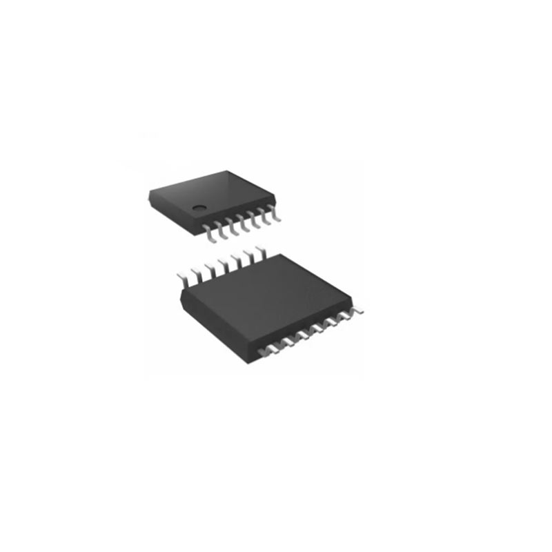
The new SSP9481 is a high-performance 80V, 1A asynchronous buck converter ideal for designing power systems with a wide range of input voltages (4.5V to 80V) and 1A on-load capability.
Below, we will elaborate on how to use the SSP9481 chip to complete 40V~60V input, 3.3V output, load capacity of 800mA power supply design tasks, including the selection of key parameters of the chip, circuit design, component selection and performance optimization.
According to the Datasheet, we can understand that the characteristics of SSP9481 meet the requirements of parameter selection.
Features:
- Output 1A persistent current, 1.5A peak current
- Input Voltage Range:4.5~80V
- 1Ω internal power MOSFET
- 480KHz fixed switching frequency
- Stable with Low‐ESR Ceramic Output Capacitors
- Cycle-by-cycle current-limiting protection
- Thermal shutdown protection
- >92% efficiency
- Output from 1V to 0.95×Vin adjustable
- Low shutdown mode current: <1μA
- SOT23-6 package
The following is a typical application diagram of the SSP9481 (output voltage is 5V), the specific content can be simplified into the input part, the control part, the output part and the feedback part. Input part: Capacitor C1; Control part: SSP9481 chip and bootstrap circuit C2; Output part: diode D1, inductor L1, capacitor C3; Feedback: resistors R1, R2 and capacitors C4.

Typical application diagram
Pin Configuration:

Chip pin diagram
BST: The pin end of the bootstrap capacitor, which internally raises the positive power terminal of the high-side MOSFET driver tube. Connect a booster capacitor between the pin and the SW.
GND: GROUND Pin
FB: Feedback input
SW: Switching pin, need to be connected to a low VF Schottky diode nearby to the ground to reduce switching spikes.
VIN: Power supply pin, and connect a capacitor to store energy and decouple
EN: Drive this pin to a logic-high to enable the IC.
Absolute Maximum Ratings
| Parameter | Range |
| Supply Voltage (VIN) | -0.3V~85V |
| Switch Voltage (VSW) | -0.3V~VIN(MAX)+0.3V |
| BST to SW | -0.3V~6.0V |
| All Other Pins | -0.3V~6.0V |
| Continuous Power (TA=+25°C) | 0.568W |
| Junction Temperature | 150℃ |
| Lead Temperature | 260℃ |
| Storage Temperature | -65℃~150℃ |
| Junction-to-Ambient THermal Resistance (θJA) | 220℃/W |
| Junction-to-Case THermal Resistance (θJC) | 110℃/W |
Recommended Operating Conditions
| Parameter | Range |
| Supply Voltage (VIN) | 4.5V ~ 80V |
| Switch Voltage (VSW) | 1V ~ 0.95*VIN |
| Operating Temperature | -40℃~85℃ |
Note 1: The maximum limit means that the chip may be damaged if it exceeds the working range. There commended operating range refers to the range within which the device functions normally, Electrical parameters define the specifications for the DC and AC parameters of the device within its operating range and under test conditions that ensure specific performance indicators.
2.Capacitor selection
2.1 Input capacitance selection
The main purpose of the input capacitor is to store energy and filter, so as to prevent the external power supply module from failing to supply power when the output requires a large current, resulting in a drop in output voltage.
Input capacitors can be electrolytic, tantalum, or ceramic capacitors, and need to add a small ceramic capacitor (0.1μF) to place the chip input pin nearby. When using ceramic capacitors, make sure they have sufficient capacitance values to prevent the input from excessive voltage ripple.
According to the design requirements, ILOAD is the output current 0.8A, fs is the switching frequency 480KHZ, C1 is the input capacitor, Vout is the output voltage 3.3V, VIN is the input voltage 40V~60V, and the input capacitor can be electrolytic, tantalum or ceramic. When the input voltage is high, it is recommended to use aluminum electrolytic capacitors as input capacitors, which can effectively alleviate the input voltage spike caused by hot swap power-up. In order to reduce potential noise, when using electrolytic capacitors, a small X5R or X7R ceramic capacitor should be placed as far as possible. For example, a 0.1uF/100V chip ceramic capacitor filters out high-frequency signals from the input DC voltage.
In this example, 47μF/100V+100nF/100V is used as the input capacitor.
2.2 Inductance selection
The main function of the output inductance is to stabilize the output current and energy storage. The LC filter circuit composed of the output inductance and output capacitance is mainly used to smooth the output voltage, so that the output voltage is a stable DC. When selecting the output inductance, in addition to considering the size of the inductance value, it is necessary to consider the current value that the inductance can inhibit. The current rating for the output inductance of the BUCK switch converter is at least 1.2 times the output current. The inductive ripple current (ΔIL) is 30% of the load current. For most designs, the inductance value can be obtained by the formula:
Formula:

According to the formula, the inductor L can choose 22μH, and the rated current of the inductor is 1A
2.3 Output capacitance selection

L is the output filter inductance, RESR is the equivalent series resistance value of the output capacitor, and COUT is the output capacitance value. For the switching power supply module, the power supply itself will produce a power ripple consistent with the switching frequency, always superimposed on the power output. The output ripple will also be caused by the internal resistance of the output capacitor, constantly charge and discharge the output capacitor, and the charging current will have a voltage drop at both ends of the RESR of the output capacitor, which will produce output ripple. Therefore, when selecting the output capacitor, try to choose the chip ceramic capacitor with smaller RESR instead of the electrolytic capacitor. Several capacitors are also selected in parallel to reduce the output impedance. The response of the control loop is faster (COT), the switching frequency is higher, or the load is not changing much with ceramic capacitors.
There are some differences between the different types of capacitors, and for ceramic capacitors, the impedance at the switching frequency is determined by the capacitance. Output voltage ripple is mainly caused by capacitance, for simplicity, output voltage ripple can be estimated by the following formula:

According to the formula calculation, the output capacitance is 2*22uF/10V+0.1uF/50V, and the output ripple is about 13mV (peak-to-peak value)
3.Schottky diode selection
When the upper tube switch is off, the output diode is an inductive current. Use Schottky diodes to reduce the loss caused by diode forward conduction voltage and reverse recovery. The average current flowing through the diode can be estimated according to the following formula:

When choosing the voltage of the Schottky diode, the reverse breakdown voltage VR should be greater than 20% to 30% of the maximum input voltage, and the higher the voltage the better, the greater the forward voltage drop VF of the Schottky diode with the increase of the voltage.
To sum up: in this example, we can choose the Schottky diode SS18
4.Feedback resistance selection
With the selection of a feedback part resistor, the SSP9481 forms a closed-loop circuit by connecting an external feedback resistor, thus stabilizing the output to a set output value. The feedback voltage is obtained through the partial voltage of R1 and R2, and the typical voltage value of VFB is 0.812V.


Reference resistance for each output voltage
| Vout(V) | R1(KΩ) | R2(KΩ) |
| 1.8 | 64.9(1%) | 80.6(1%) |
| 2.5 | 23.7(1%) | 49.9(1%) |
| 3.3 | 16.2(1%) | 49.9(1%) |
| 5 | 23.7(1%) | 124(1%) |
Use the resistance values recommended in the manual.
5.Final schematic diagram

6.Layout design
(1) The Vin capacitor should be placed near the Vin pin of the chip and the signal ground of the chip, as far as possible in one layer, because the input current is discontinuous, and the noise caused by parasitic inductance has an adverse effect on the voltage resistance of the chip and the logic unit. The smaller the loop of the high-frequency loop, the smaller the magnetic field energy.
(2) FB is the most sensitive and easily disturbed part of the chip, and is the most common cause of system instability:
- The FB resistor is connected to the FB pin as short as possible to reduce noise coupling.
- Away from noise sources, SW points (switching nodes), inductors, diodes (non-synchronous buck).
(3) Placing the inductor does not need to be as close to the IC as placing the input capacitor to minimize the radiated noise of the switching node. Generally, it is not recommended to lay copper under the inductor, because the eddy current in the ground layer will cause the inductance to decrease.
(4) The output filter capacitor is as close to the inductor as possible. The smaller the loop of the high-frequency loop, the smaller the magnetic field energy.

Figure 2.2
(5) The SW point is the noise source, which ensures the current while keeping the area as small as possible, away from the sensitive and easily disturbed position. Reducing the area of the node and replacing the inductor with a smaller volume can reduce the electric field strength, as shown in the figure:

7.Test
Input voltage test
The equipment used in this test are: Puyuan brand MSO5204 digital oscilloscope and multimeter.
Oscilloscope ripple test Settings:
Coupling mode: AC coupling,
bandwidth limit: 20M, pen: X1.
Test with ground springs.

Universal source MSO5204 digital oscilloscope
The following figure shows the test diagram of the output voltage power-on. It can be seen from the oscilloscope that the maximum output voltage is 3.40V, the rising edge of the output voltage is gentle, and there is no ringing and voltage overshoot.

Output voltage power-on test
The following figure shows the ripple of the output voltage when the input voltage is 40V and the load is 800mA. It can be seen from the oscilloscope that the peak-to-peak value of the ripple is 14.25mV

Output ripple test chart
The following figure shows the ripple of the output voltage when the input voltage is 60V and the load is 800mA. It can be seen from the oscilloscope that the peak-to-peak value of the ripple is 17.42mV

Output ripple test chart
From the actual test waveform, the output voltage ripple peak is very close to the calculated result.

